
We’re still in a lull before Q2 2024 earnings season begins in earnest, which gives us time to explore fun little research projects – and come to a deeper understanding of an often-explored part of the semi industry: Manufacturing equipment.
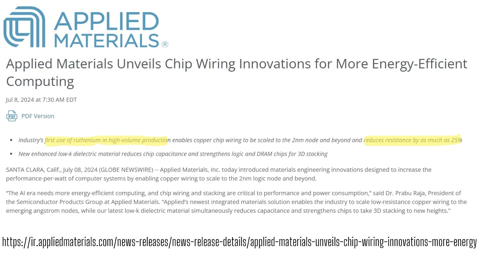
Earlier in July, Applied Materials (AMAT) quietly announced a new breakthrough in wafer-level packaging that could be a key to continued scaling of chips to 2nm and smaller (of course 2nm referring to, not so much the transistor size, but the equivalent performance increase relative to past manufacturing processes).
What is this new revolutionary process that could be big news in this new AI era? First, a high level recap.
Not just scaling smaller…
By now, everyone has probably heard the semiconductor industry is on a path (or at least hopes it’s on a path) towards reaching $1 trillion in global end-market sales by 2030. This implies an expected compound annual growth rate (CAGR) of over 9%!

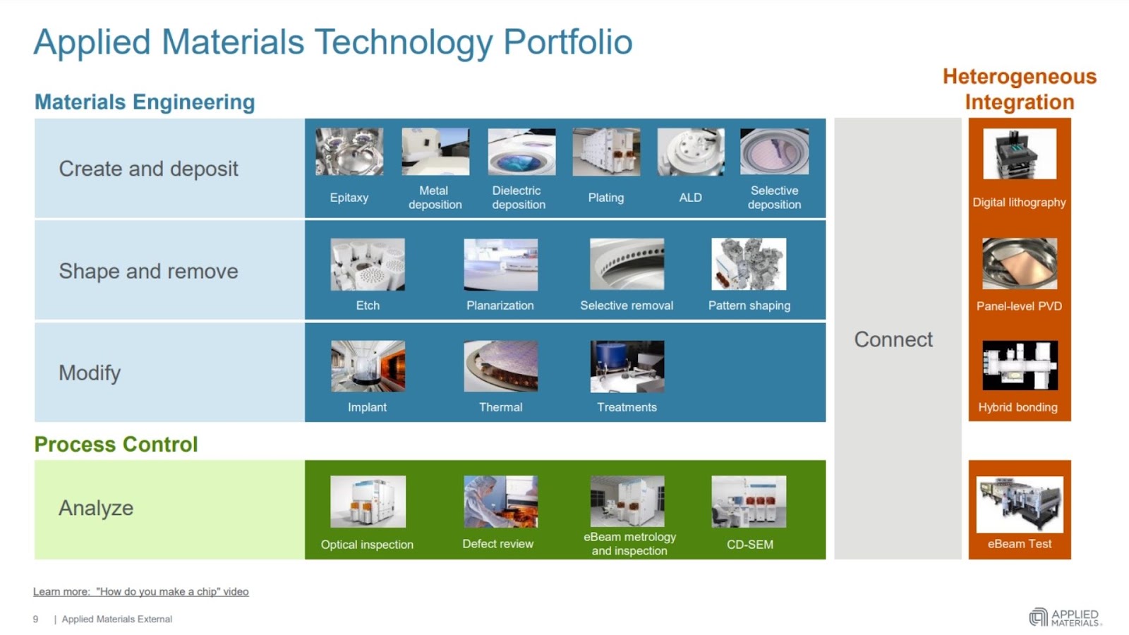
But to get there, existing semiconductor manufacturing will need to continue to advance. As electronics proliferate every corner of the economy, manufacturing processes are getting tailor-fit to end applications to boost performance. Applied has been talking about this for years regarding its work in materials science for advanced substrates and packaging techniques.
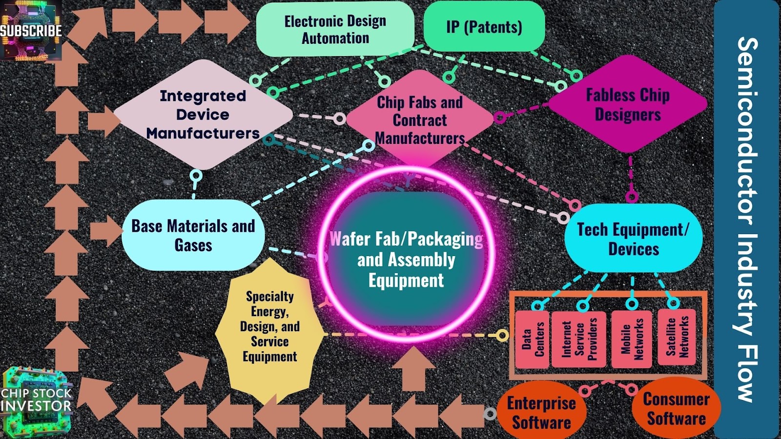
This means great things for the manufacturing equipment providers, especially the “Fab 5” (Applied, along with ASML, Lam Research, Tokyo Electron, and KLA Corp).
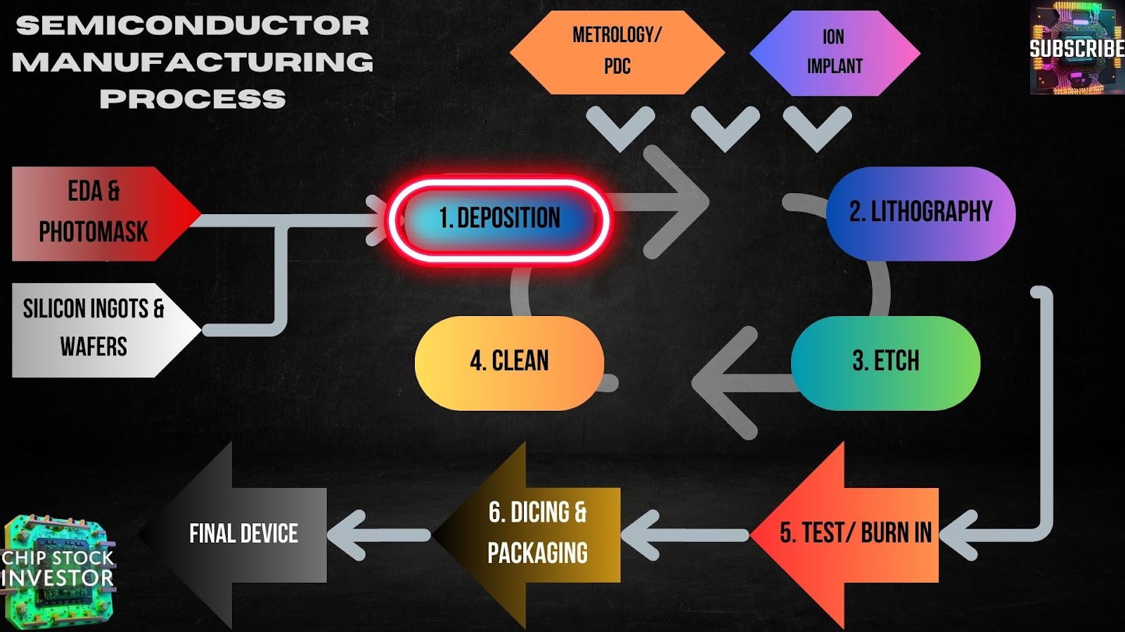
One specific process that is changing is deposition, a catch-all for a number of methodologies for depositing thin films (or layers) of conductive and insulating material atop the silicon wafer substrate.
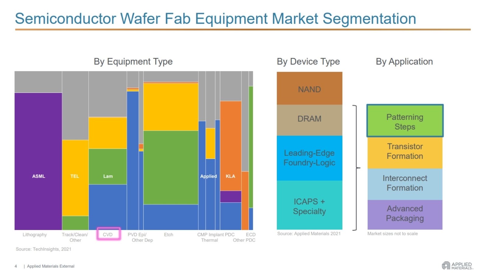
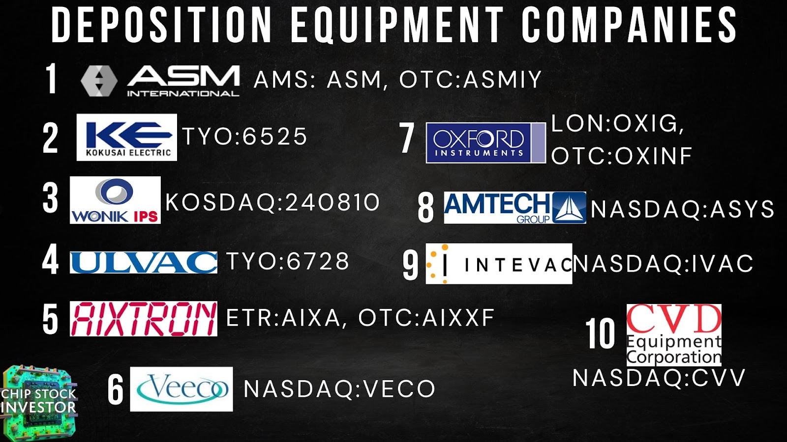
Applied, along with Lam and Tokyo Electron, and some specialists in deposition like ASM International, are dominant forces in deposition. See the market share bar circled CVD below (CVD = chemical vapor deposition).
These thin layers of conductive and insulating material build up a type of microscopic 3D city on the surface of the wafer, a complex of tiny towers and trenches that act as the conduits and drains for electricity – which in turn act as the on-off switches that form the basis of software code.

Applied’s new deposition breakthrough
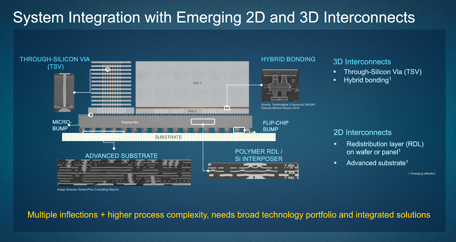
Which brings us to Applied’s innovation for chip wiring, a wafer-level packaging technique. At the turn of the millennium, Applied helped pioneer what is today the industry standard of wafer-level wiring: Copper.
You may be thinking, well of course copper is standard for wiring. Surprise, though, it wasn’t always that way. At the microscopic level, copper wiring does funny things that creates issues with resistance and capacitance. The big manufacturing equipment generalist developed a CVD method for applying a low-k dielectric film that helped solve this problem with copper wiring that stitches together those “3D cities” on the surface of silicon substrates. TSMC was a quick adopter of the tech, which helped it soar into the consciousness of the semi community, and begin the slow process of passing up long-time tech leadership of Intel when it was still in its heyday.
This is technical stuff for chemists and physicists, but if you want a great overview of that, check out Asianometry’s video on the subject about nine months ago. Asianometry is awesome TV. TSMC’s First Breakthrough: The Copper/Low-K Interconnect Transition
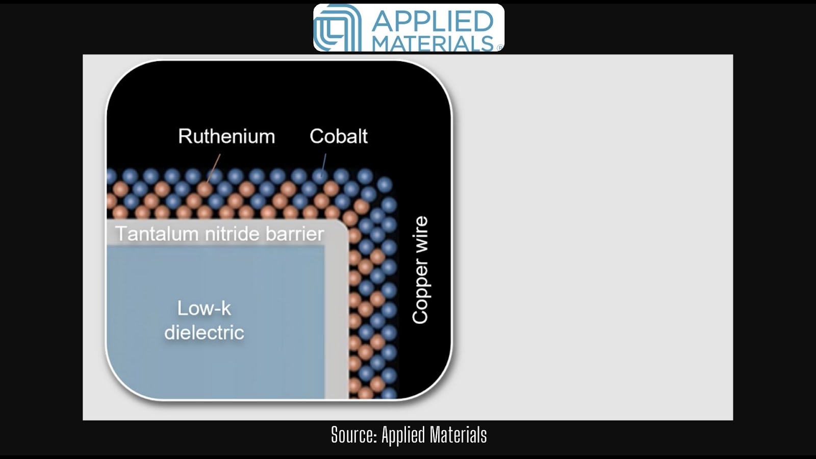
Applied is at it again, though, innovating a new layer of ruthenium – a first for the element in high-volume production – on top of the low-k dielectric layer that further improves the efficiency of itty-bitty copper wiring.
Wait, layers of… ruthe-what?
Applied provided some micro-level cross-sections of what all these new layers look like. First, a look at its trademarked Black Diamond low-k dielectric film and how it’s layered with the copper wiring interconnects.
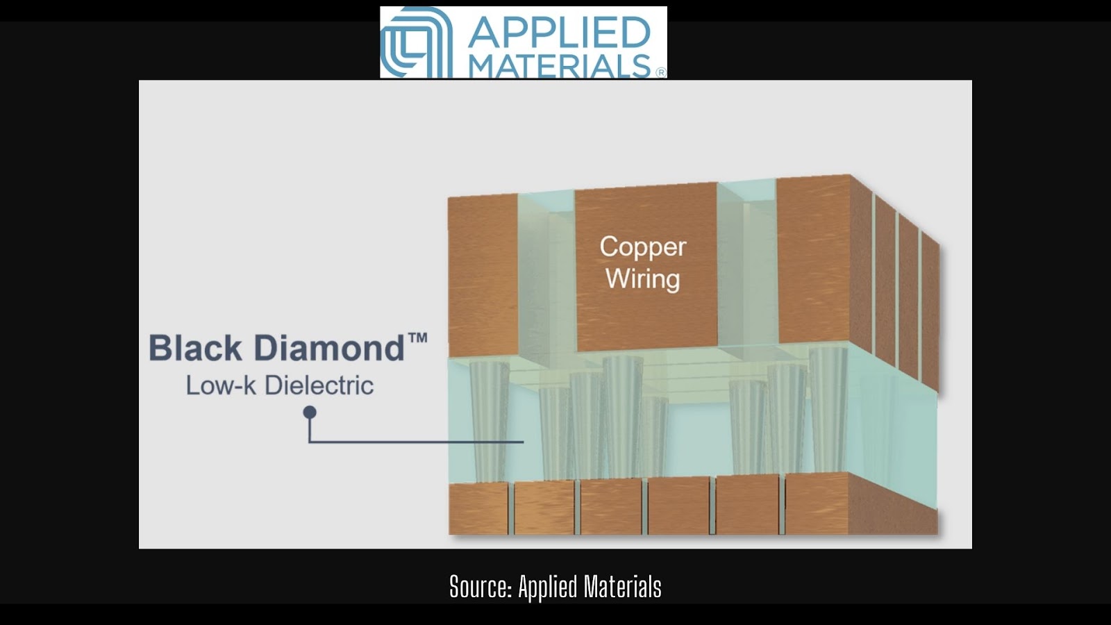
The new innovation involves a new generation of low-k dielectric film chemicals, but the real breakthrough is in new types of “barrier” layers between the low-k dielectric and the eventual copper that’s filled in between it.
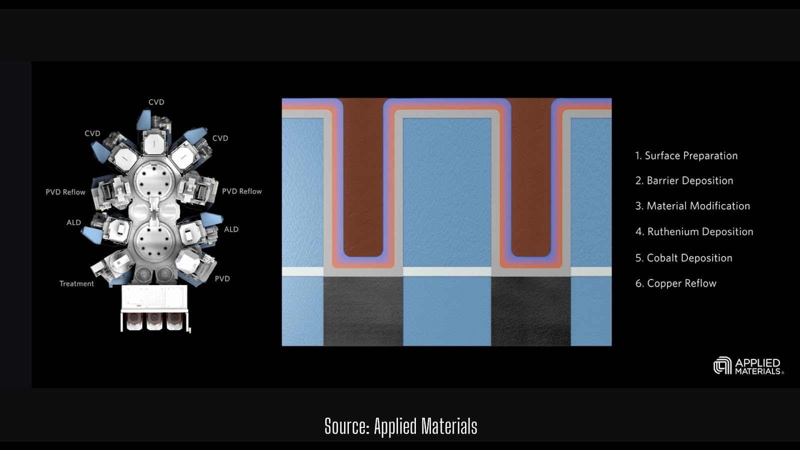
As you can see from the process steps above, a thin film of ruthenium and then cobalt are placed before the copper wiring, enabling the copper fills to scale to smaller sizes (2nm and below) by solving for some of the resistance-capacitance issues that crop up with copper at that tiny of size.

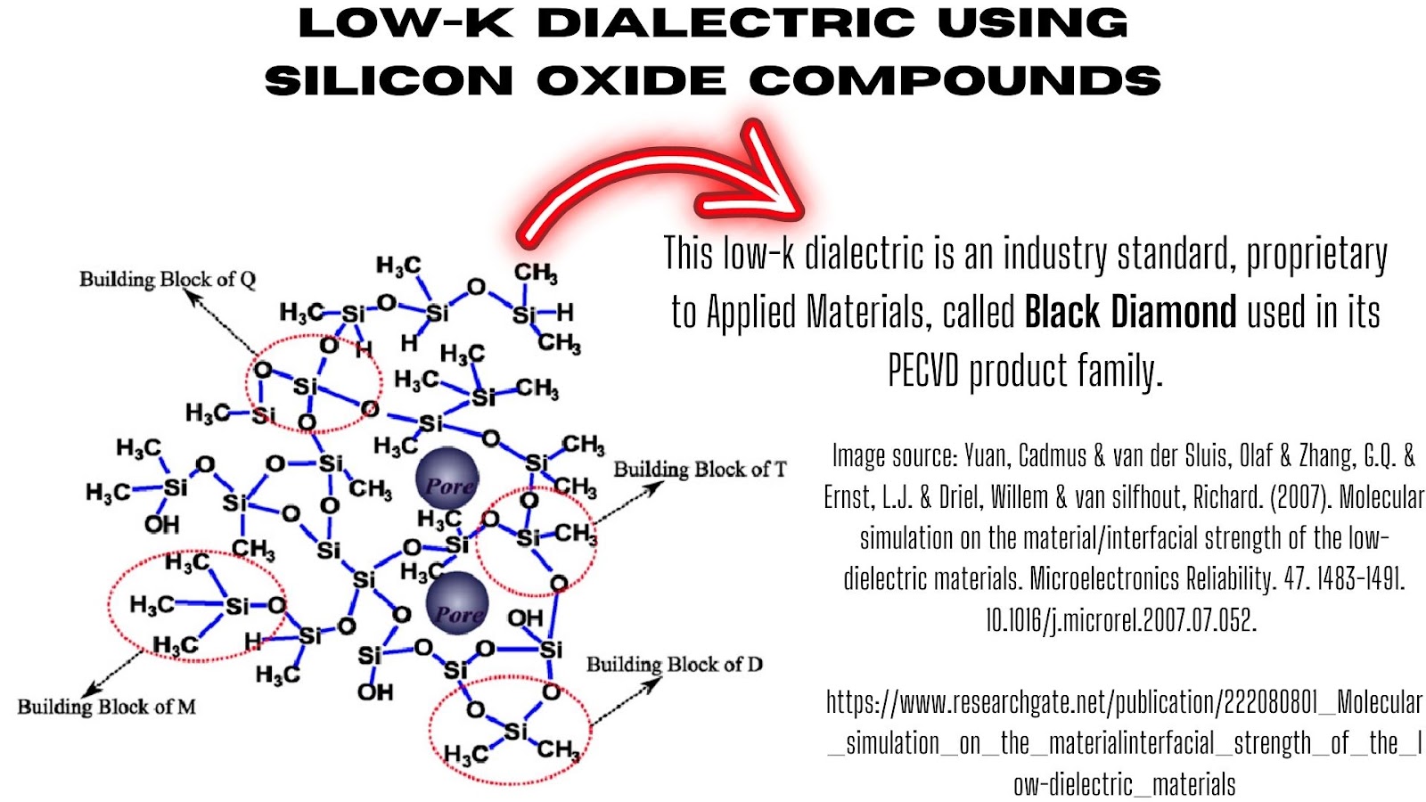
All of this is put in place using PECVD, or “plasma enhanced” CVD, using plasma (ionized gas) particles of the elements ruthenium and cobalt on top of the traditional silicon oxide-based Black Diamond low-k dielectric Applied has been supplying the chipmaking industry for decades now.
Applied says that all the advanced node chipmakers are adopting its new process step to help with chip scaling at 2nm and below. This likely means Applied has TSMC, Intel,and Samsung already wrangled, and memory chipmakers like SK Hynix and Micron perhaps in the works for later on. Great news for Applied’s deposition steps – a staple of the company’s sales. Here’s a video of the process from Applied:
Applied Materials’ Chip Wiring Innovation Enables More Energy-Efficient Computing
I slept through chemistry, what is ruthenium?
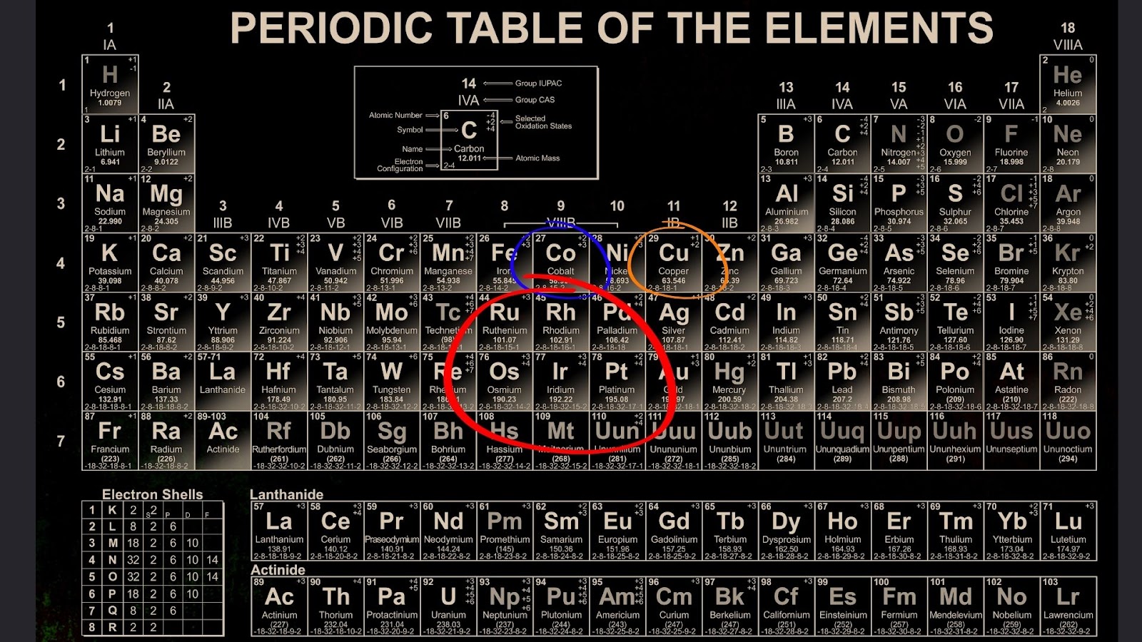
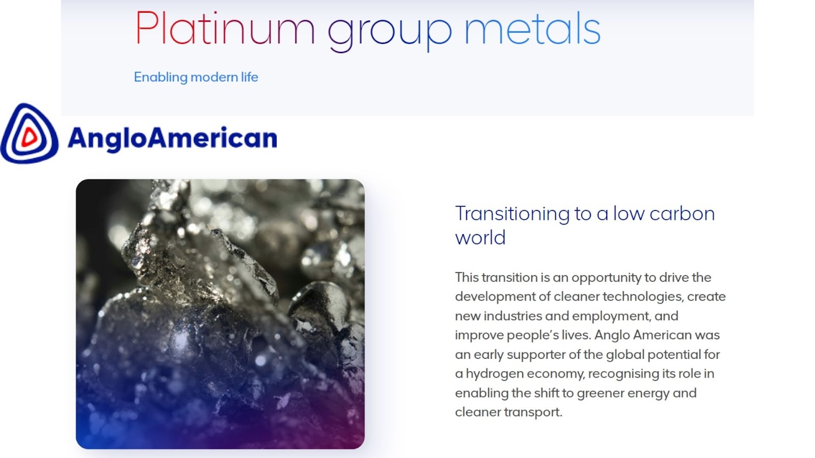
The first question we had in reading this report was: What the hell is ruthenium?
For those of us that aren’t chemists, or strange people that like reading the periodic table, ruthenium is a member of the “platinum group metals” – the six elements including platinum, palladium, iridium, osmium, rhodium, and of course the star of this episode, ruthenium.
Second question, where would Applied even find such a niche sounding metal? Doing a brief search online, it was no surprise to find top platinum producers like Anglo American surface to the top. It seems Sibanye Stillwater also is a ruthenium supplier, but they were suffering a ransomware attack this past week… ?

If you’re interested, Nick put together a list of various metal miners a few years back, including platinum, using an enterprise AI research tool called noonum.ai. The public list of those can still be found here: https://www.fool.com/investing/stock-market/market-sectors/materials/metal-stocks/platinum-stocks/
Also of note, while Applied isn’t a chemicals supplier directly, the business is deeply entrenched in developing special manufacturing materials and supply chain solutions for the electronics industry. Given this is a core holding in our portfolio, it’s one of the key reasons why we opted to invest in Air Products and Chemicals (APD) last year, given its natural gas liquefaction business (which is now unfortunately being sold to Honeywell) instead of the more focused chemicals bet Linde. But that’s a different story.
Ok, so how do these microscopic layers of elements I’ve never heard of get deposited?
Let’s now introduce Applied’s latest marvel in CVD. Along with the new ruthenium layer process, the Applied Endura CuBS IMS with Volta Ruthenium CVD (what a mouthful, that’s not going to win any product naming awards) was announced.
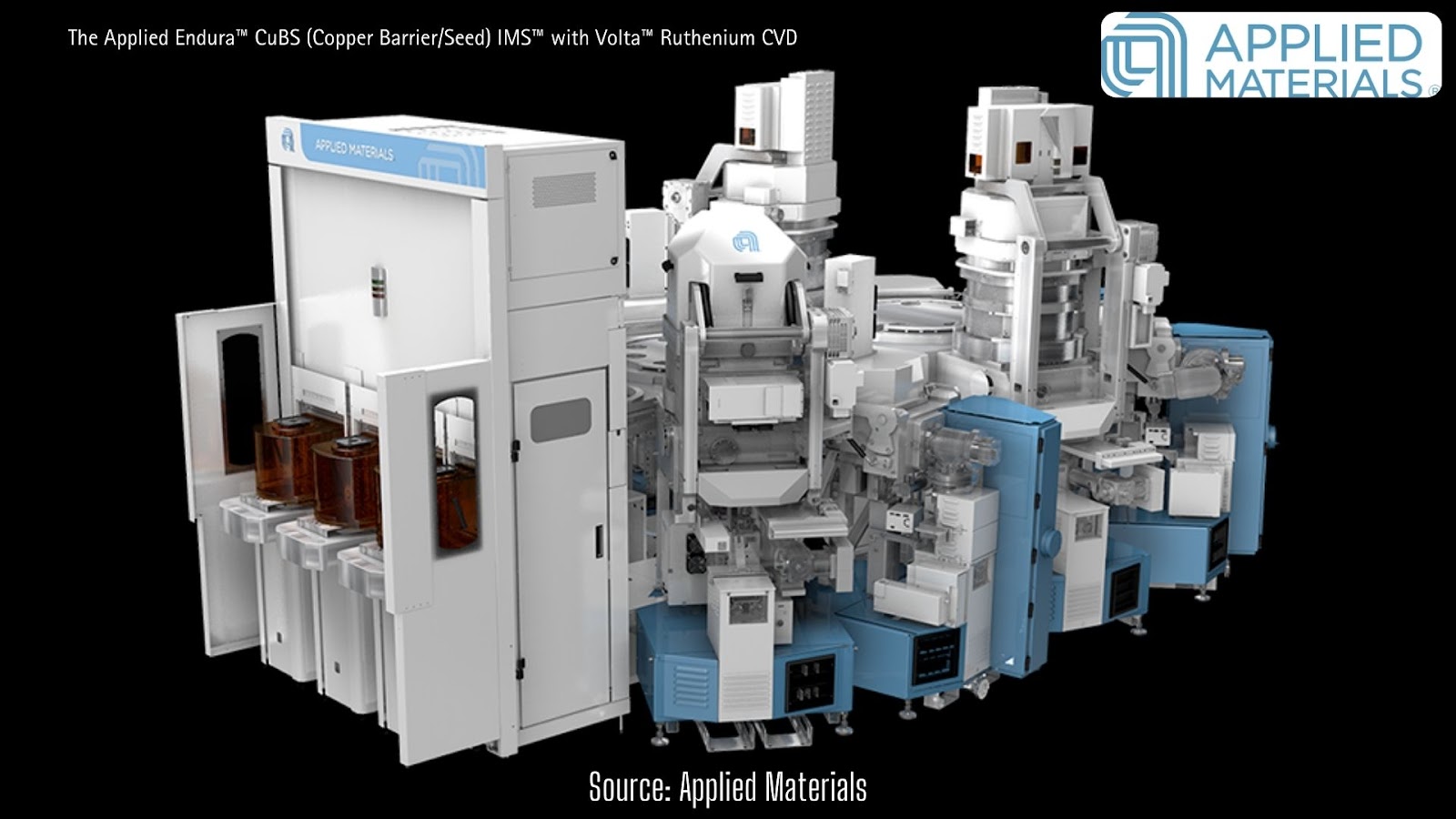
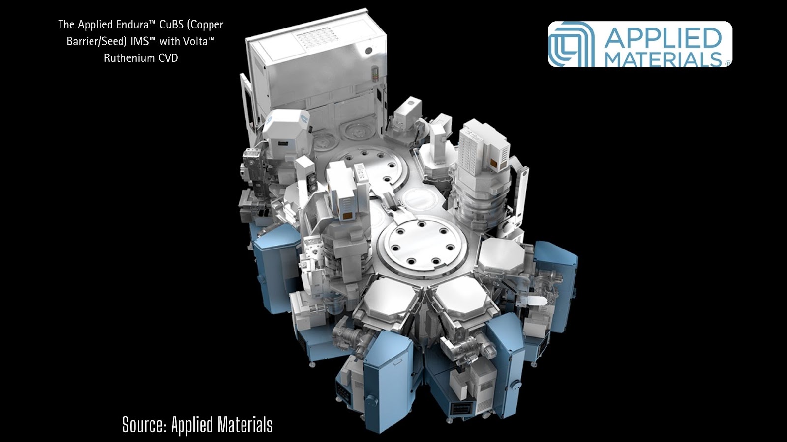
What this behemoth equipment lacks in catchy naming it makes up for in fab space utilization. It combines six different manufacturing technology process steps into one piece of machinery (thus the multiple vacuum chambers oriented in a semi-circle in the images above). Applied said all the major logic chipmakers began receiving orders of the machine when they began work on their 3nm nodes, probably so they could begin testing the machine while developing 2nm processes that will begin production in the next couple years. https://ir.appliedmaterials.com/news-releases/news-release-details/applied-materials-unveils-chip-wiring-innovations-more-energy
The power of manufacturing equipment
Innovations like this one are obviously going to be key for companies like TSMC, Intel, and Samsung, as advanced packaging will be critical to push the performance boundaries of AI systems and the chips used to power them. But it also speaks to the power of the equipment providers themselves. While the advanced fabs often get all the credit for developing and manufacturing the chips themselves, it’s actually the Fab5 and smaller peers quietly working behind-the-scenes making all of these tech breakthroughs possible in the first place.
And for investors looking for tech businesses with actual “moats,” it’s these equipment providers that have some of the strongest pipelines of growth and defensive barriers to would-be competitors. Companies like Applied are sitting on decades of innovation, protected with extensive patents and IP (like Black Diamond CVD for Applied), that have led to stellar investor total returns.

Will the same performance take place over the next seven to eight years? Maybe, but we think more likely not. But that doesn’t mean Applied, the Fab 5, and equipment providers in general won’t be top ways to play the AI supercycle. And with the whole semi industry finally poised to return to growth starting the second half of this year, a new multi-year run higher might still be in the early innings.
Applied need not be a top pick, however, there are lots of great equipment providers with strong positioning. Make sure to check out the full Wafer Fab and Chip Packaging video and manual here if you haven’t seen it yet, as well as our recent mid-year update on this sub-industry: AI Supercycle: Your Ultimate Guide To Investing In Semiconductor Manufacturing Equipment Stocks The Chip Stocks Powering the Next Leg Up of the Bull Market In 2024? AI Supercycle UpdateVideo link: https://youtu.be/fbXWO5_lvxw
