
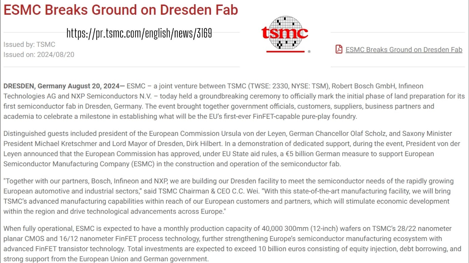
August has been a busy month for the world’s largest and most advanced foundry, Taiwan Semiconductor Manufacturing (TSM). Just the other day, the joint venture ESMC between TSMC, Bosch, Infineon, and NXP Semi broke ground in Dresden, Germany. That will eventually be a unique asset, a first-of-its-kind for Europe.
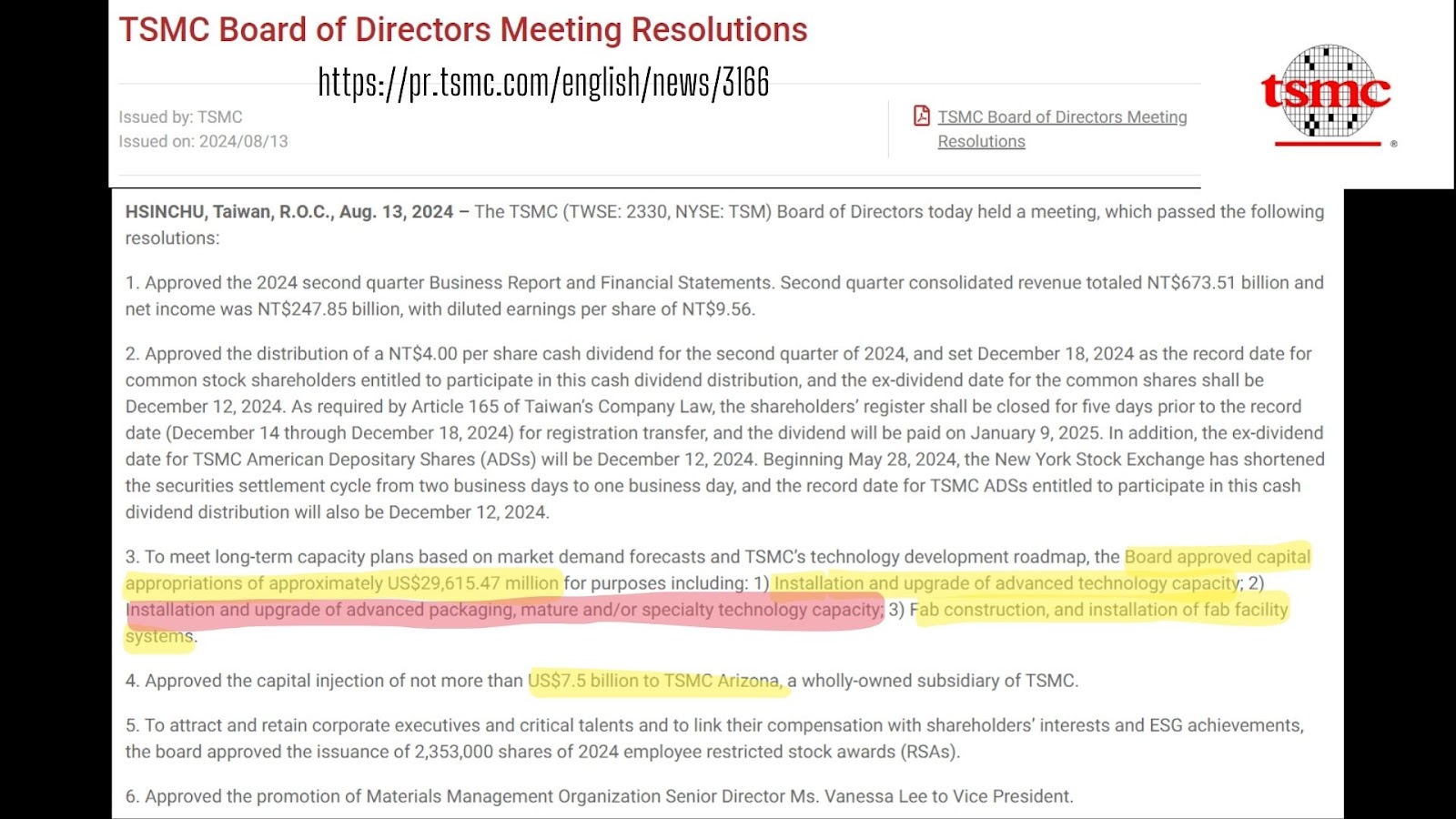
And then there was TSMC’s Board of Directors meeting, which approved nearly $30 billion in capital expenditures for the next year. Besides infusing TSMC Arizona with more much-needed capital for construction, there was an intriguing little point on “advanced packaging.”
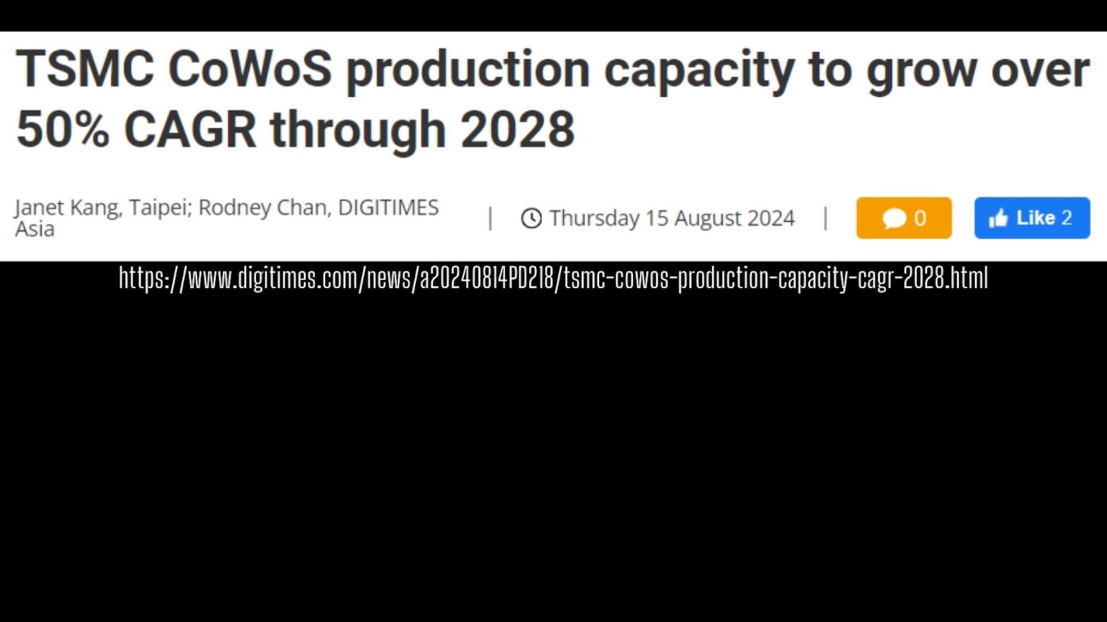
Hot on the heels of this announcement, DigiTimes said it thinks TSMC’s CoWoS (chip-on-wafer-on-substrate) advanced packaging manufacturing capacity will put up a sizzling 50% compound annual growth rate through 2028.
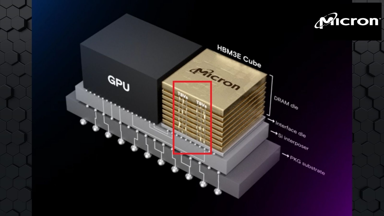
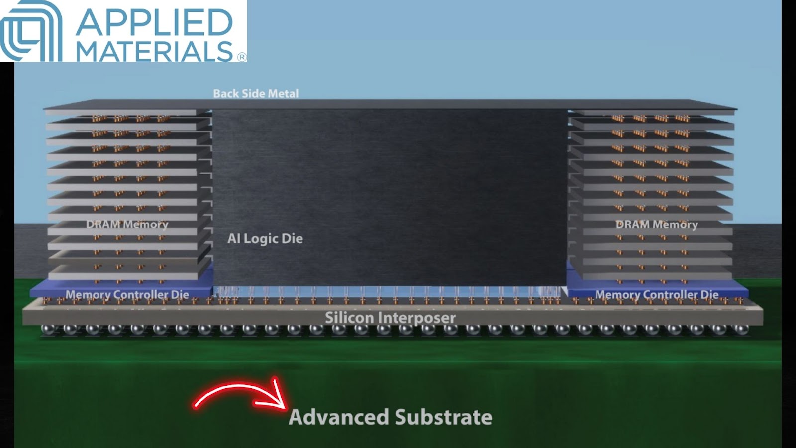
This kind of advanced packaging has paved the way for computing accelerators from the likes of Nvidia and AMD. You’re probably getting used to seeing what these look like by now. A GPU (the accelerator) with cubes of stacked DRAM (high-bandwidth memory, or HBM).
TSMC already has a few advanced packaging fabs that will likely receive a bit of that $30 billion CapEx budget in the next year.
But there’s another little tidbit of info that came out amidst all this TSMC news that sent Nick down a rabbit hole: Glass panel substrates. Does glass even mix with silicon? How does that work? Let us explain. We did talk about this glass topic a bit back in July, and included those show notes at the end of these ones.
TSMC does a little shopping
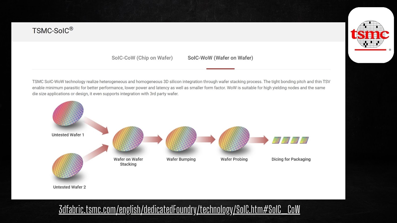
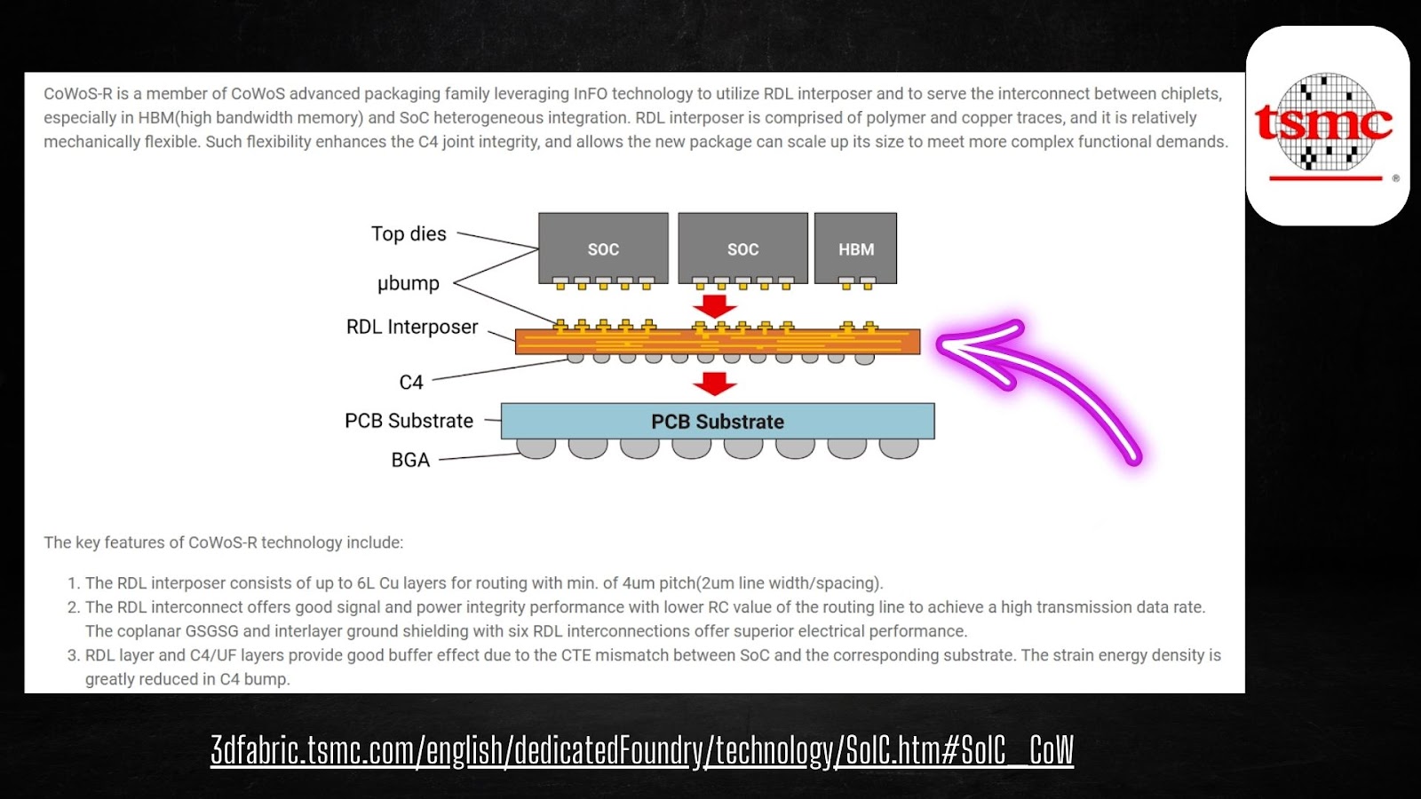
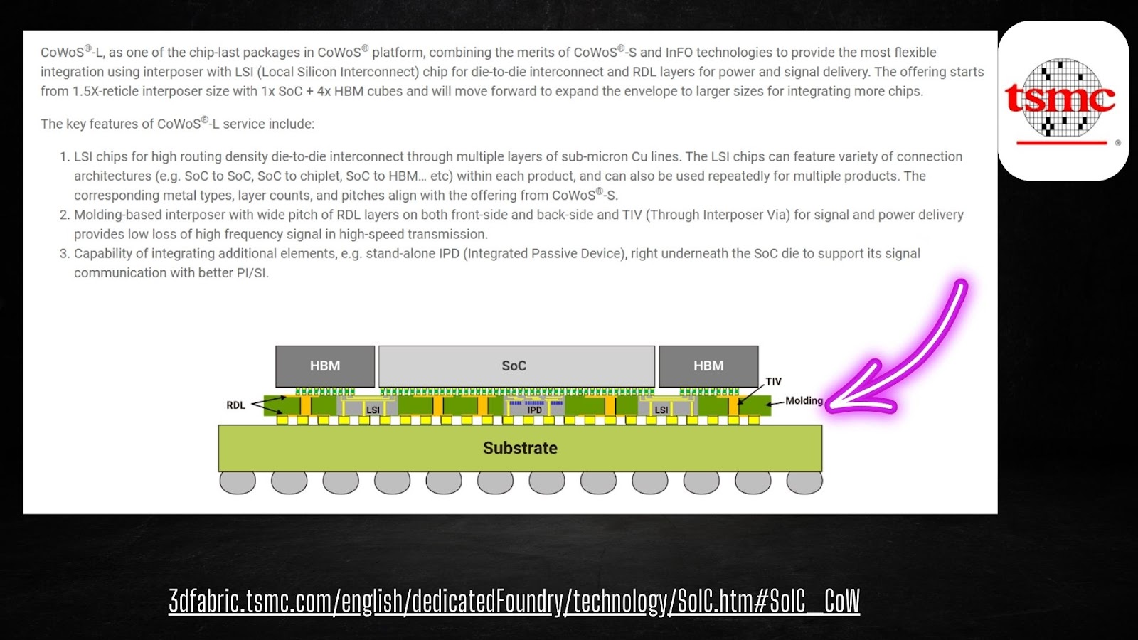
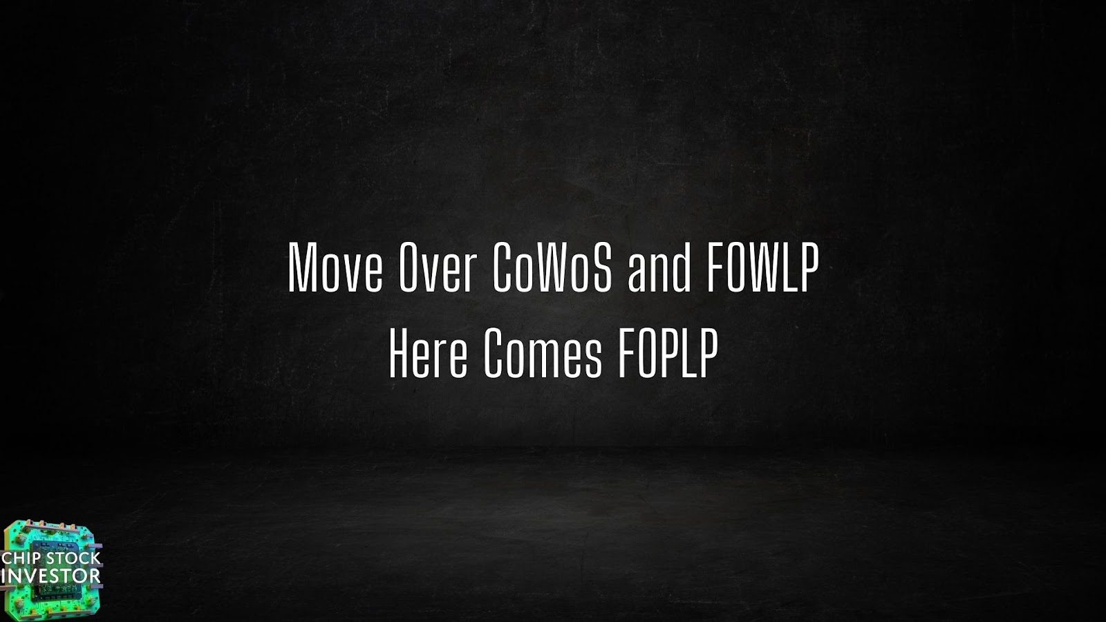
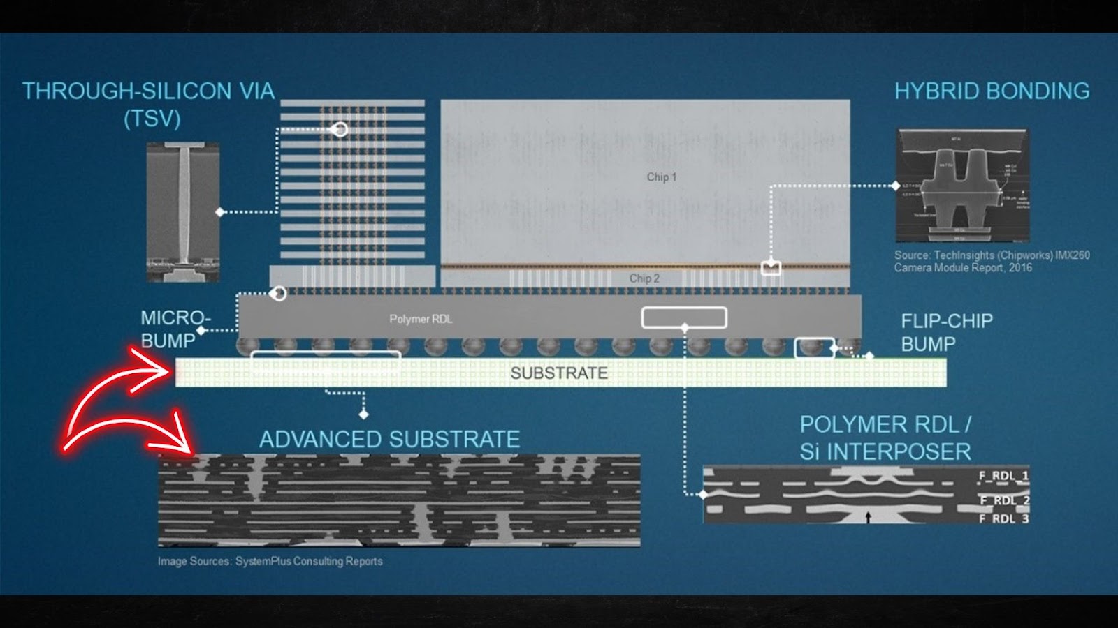
First, let’s define a few acronyms – CoWoS, FOWLP, and FOPLP. For the first two, CoWoS and FOWLP, see the previous cross-sectional images from earlier to get an idea of what this type of advanced packaging looks like.
- CoWoS: chip-on-wafer-on-substrate
- FOWLP: fan-out wafer-level packaging
- FOPLP: fan-out panel-level packaging
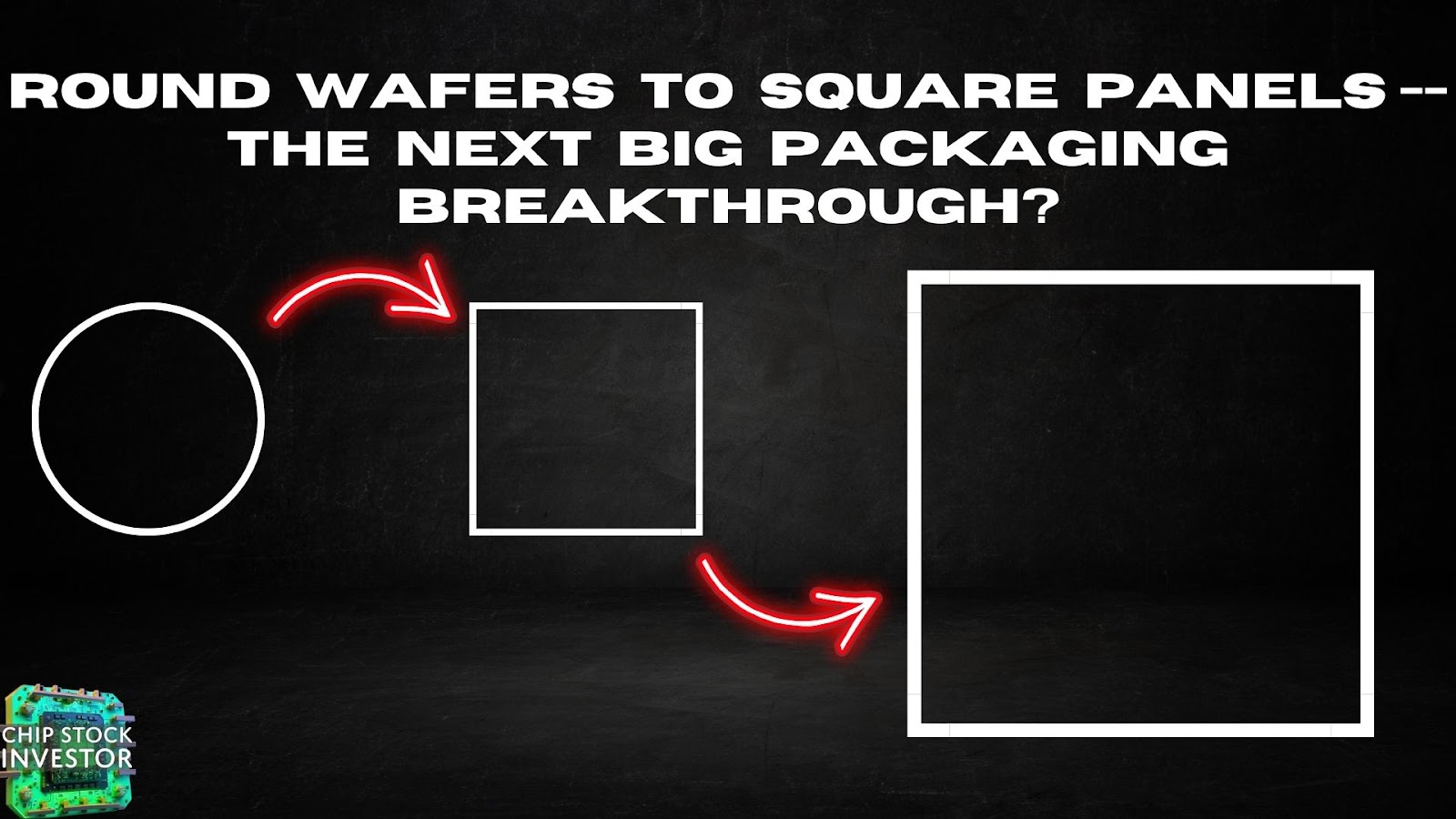
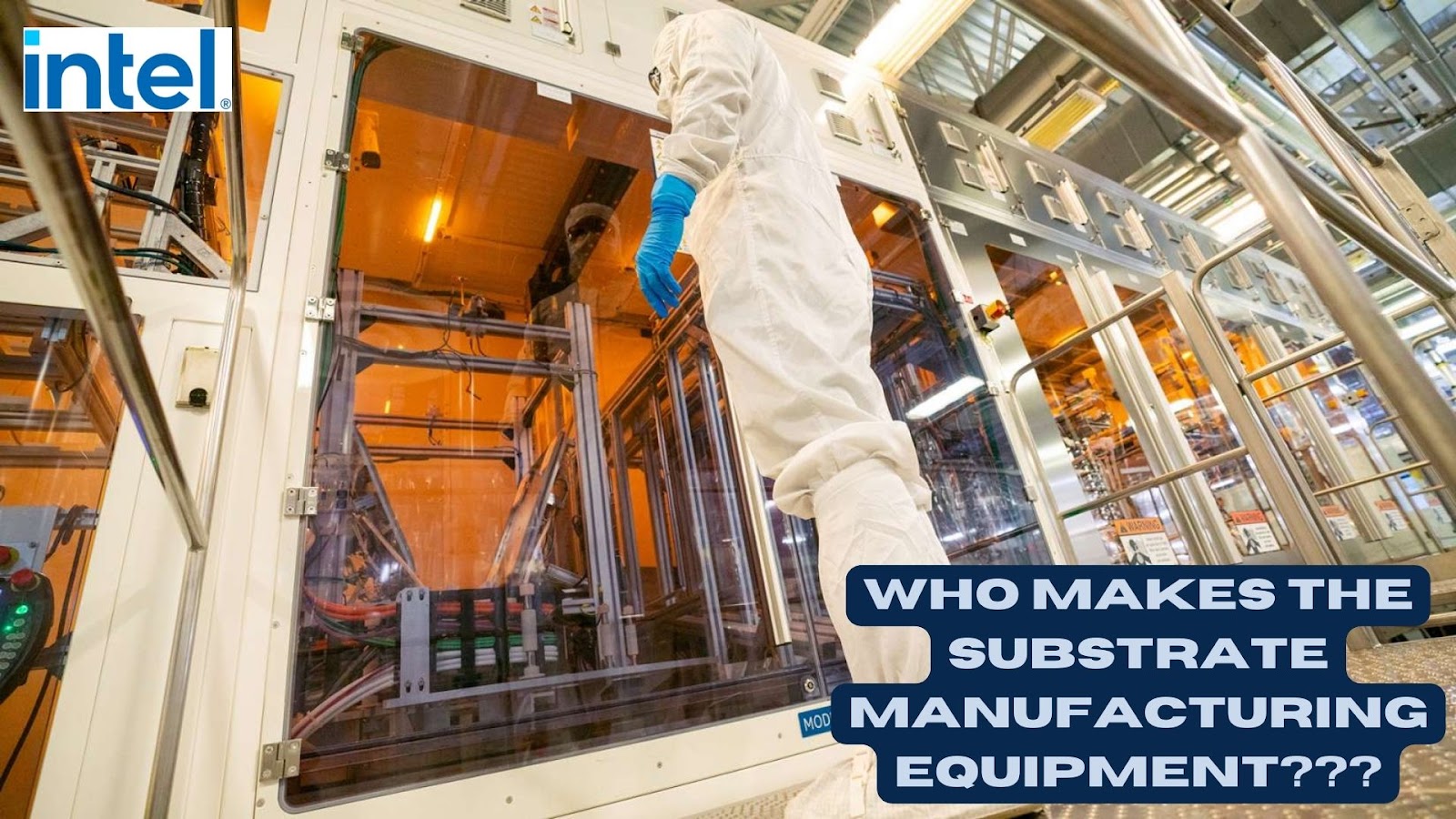
Currently, advanced packaging involves developing silicon wafers (the things that get diced into chips), and packaging them atop another silicon wafer. But with wafer development reaching its limits (see our recent coverage of ASML and Applied Materials ASML’s High-NA EUV Breakthrough: Massive Investment Returns Ahead? Applied Materials (AMAT Stock) Signals Massive AI Growth For the Next 15 Years), chipmakers are looking for other low-hanging fruit to increase computing performance in a more economical way.
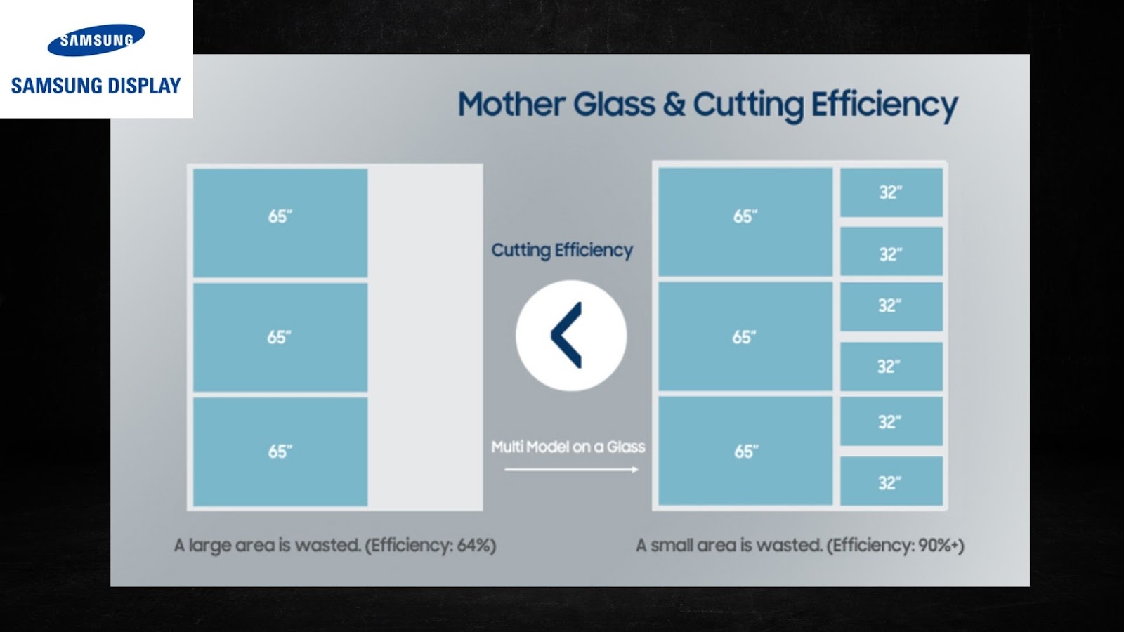
This is where focusing on the chip package itself comes in, an area of the computing system that has received minimal attention the last couple decades. That’s starting to change. To increase ultimate semiconductor device yields, chipmakers are working on making the switch from silicon wafers, to a square panel (squares have less waste at the edges, versus the edges of a circular wafer).
What’s glass got to do with it?
Amid all the TSMC news at the outset, it was confirmed that TSMC acquired an idled LCD (liquid crystal display) screen manufacturing facility from Innolux – a leading display maker in Taiwan.
TSMC of course isn’t interested in making digital displays. But it may very well be interested in the glass panels Innolux was making at this facility. TSMC bought the plant for a little over $530 million (when converted into U.S. dollars).
Innolux apparently confirmed its employees have (obviously) ample experience with glass panels, and that (less obviously) 60% of the equipment inside the facility can be repurposed for FOPLP (fan-out panel-level packaging).
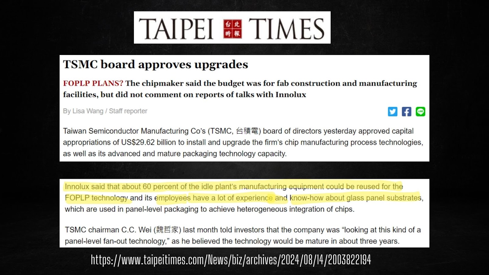
In some of its investor communications, Innolux had expressed interest in developing FOPLP advanced packaging, a technology that might be ready for next-gen computing accelerators and data center AI systems in another two to three years. But perhaps Innolux decided cashing in on this facility by selling to TSMC was a better investment return.
At any rate, what does this mean for TSMC, its shareholders, and the Chip Stock Investor community?
So… we need to know how digital displays work now
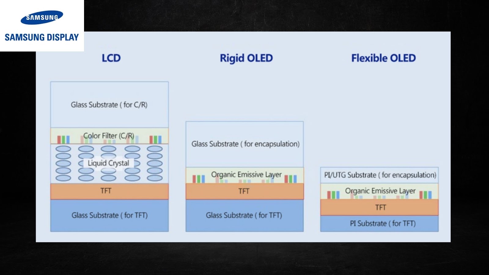
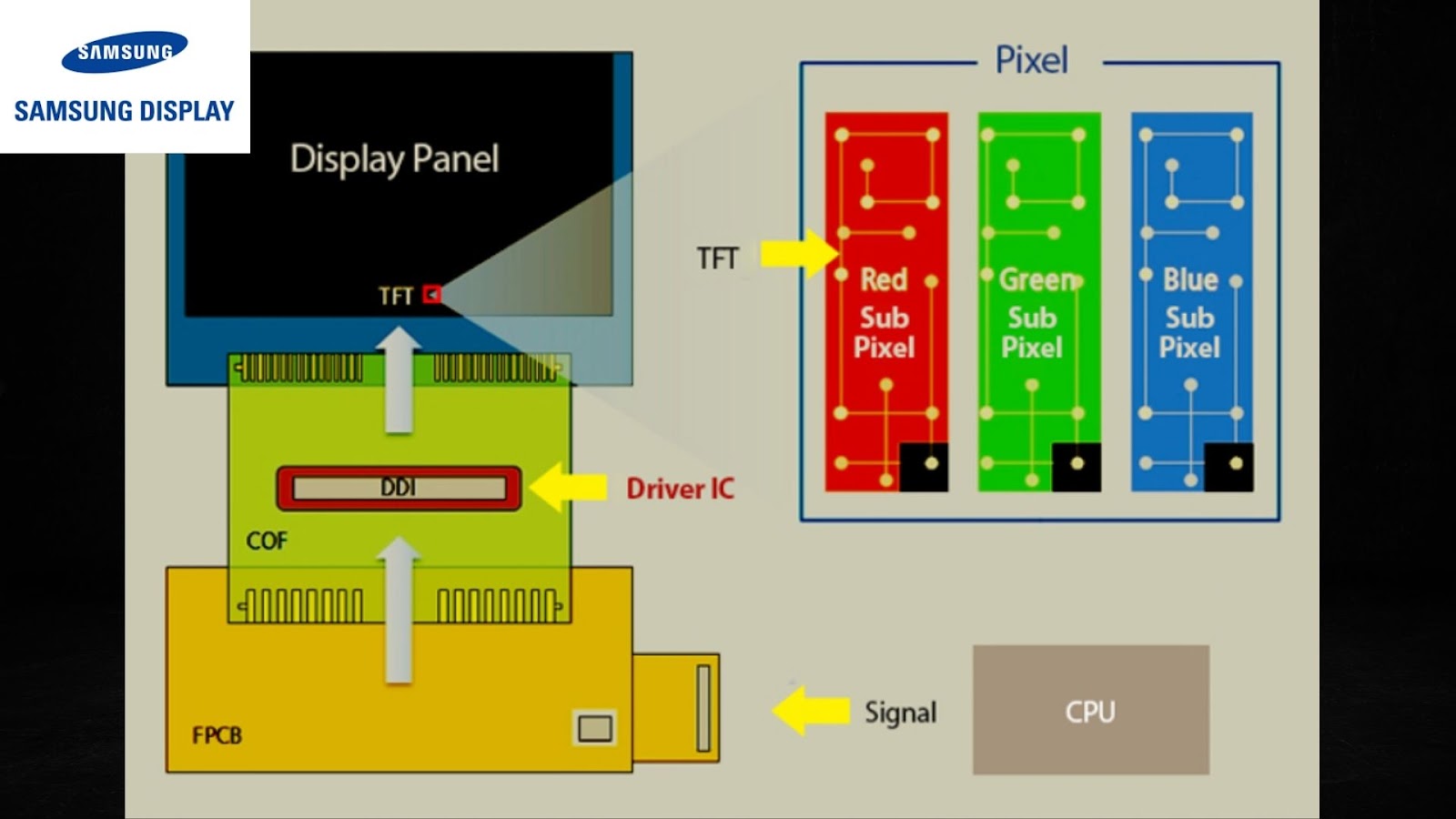
It’s been awhile since we covered it, but we shared this image from one of our CSI universe stocks, Universal Display – a patent developer in OLED (organic light-emitting diode) displays. Be it older LCD or OLED screens, a key layer to digital displays are TFTs, or thin film transistors. This is a layer of transistors (those on-off electrical switches that create the 1s and 0s in digital code) printed on a glass panel, that handles the flow of electrical current, and the ultimate control of the pixels in a digital screen.
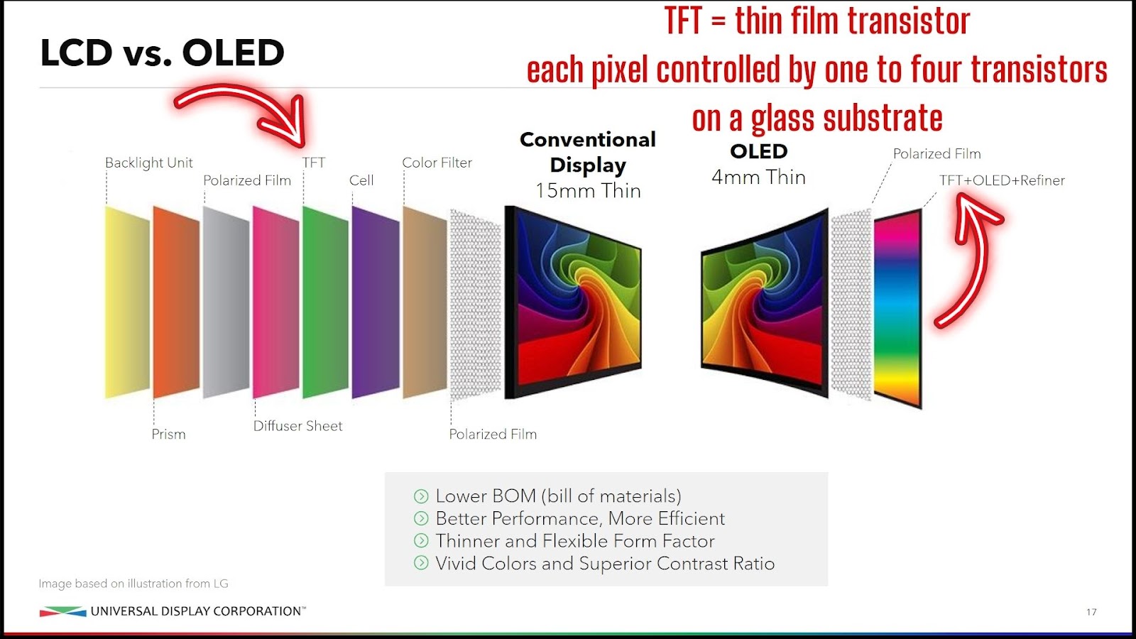
Here’s a cross-section of an LCD and OLED display, where you can see the TFT layer.
How are those transistors made? And what do they do? It starts with big sheets of thin glass, cut down to size for a TV, computer, or smartphone screen.
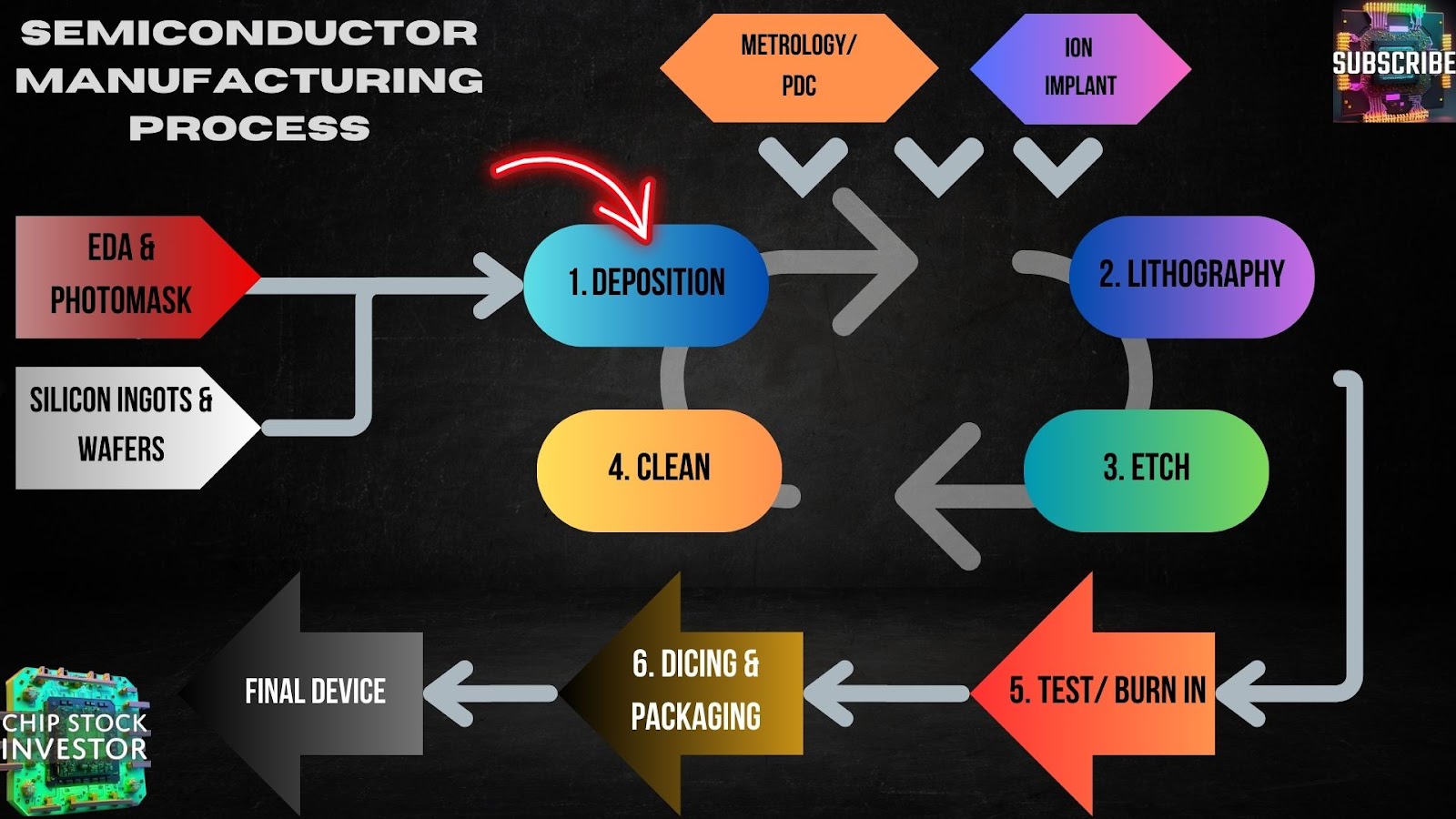
Next, you’ll recognize the following steps, the same ones involved with silicon wafer development: Deposition, lithography, etch, clean, repeat. The difference here is these steps are done on the glass substrate to create those TFTs (cross section shown on the right of the second picture below).
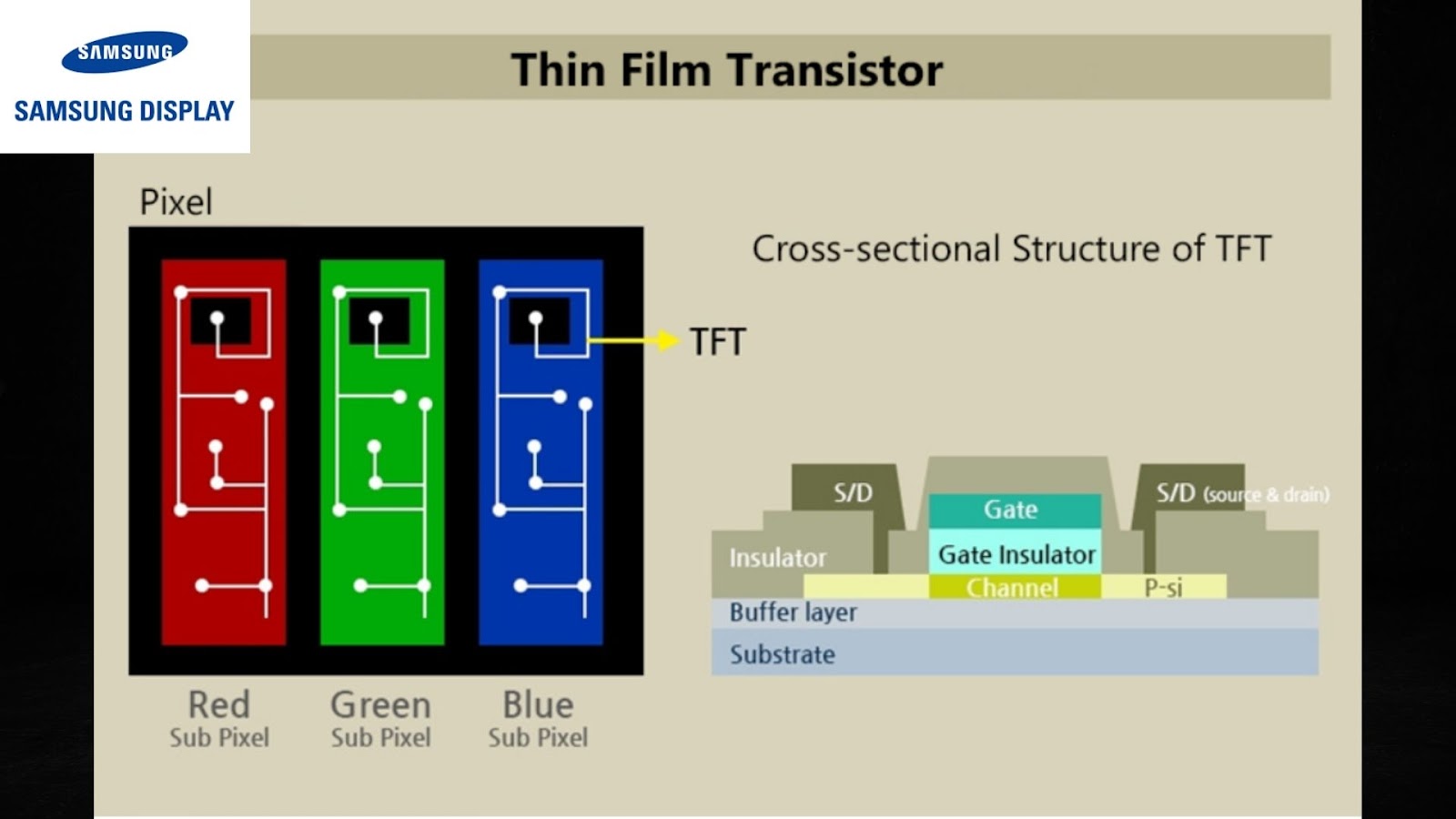
What are those transistors for? They control which color (red, green, or blue) the pixel turns in the layer above the TFT. The computer’s CPU sends the image data to the display driver (a different chip), which translates this into the TFT and ultimately the image or video you see on your display.
Cool story, but those are displays – what about advanced packaging?
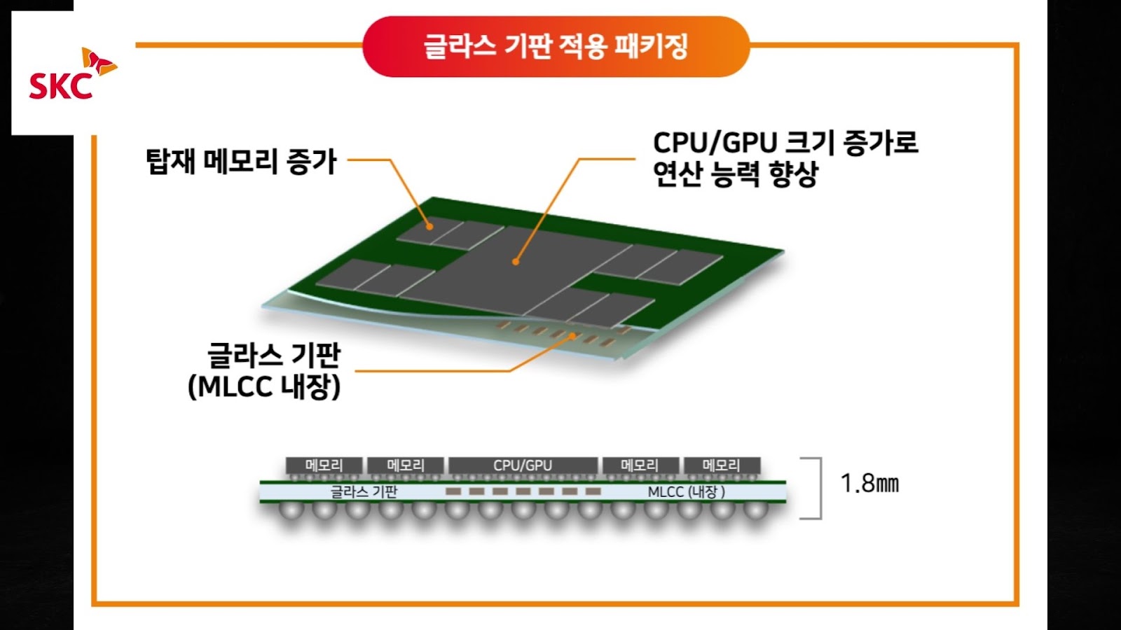
Why would TSMC, and other chipmakers like Intel, want to do all this stuff with glass, but for advanced packaging substrates (instead of for displays)? Well, glass has properties that could dramatically increase computing system performance. Digital display tech is quite efficient, and some of that efficiency might be able to bridge over to advanced packaging of logic and memory systems. Glass can help a great deal with increasing the density of input-output signals between different chips in the computing system. And it’s also a stable substrate, not prone to as much warpage, and holds up well under heat generated from electricity flowing through the copper fills in the chips.
On the downside, glass is a more fragile and brittle substrate, so that will be (and has been) a challenge for engineers looking to use it in chip packaging.
Nevertheless, it seems much can be borrowed from the LCD panel industry, as Innolux hinted (remember, perhaps 60% of the existing equipment in that fab sold to TSMC could be used in FOPLP).
Intel has also been working on FOPLP for some time. Perhaps we’re nearing commercialization of these things, especially as AI data center systems are putting tremendous demand on chipmakers to increase power-to-performance ratios.
Who will win the FOPLP battle?
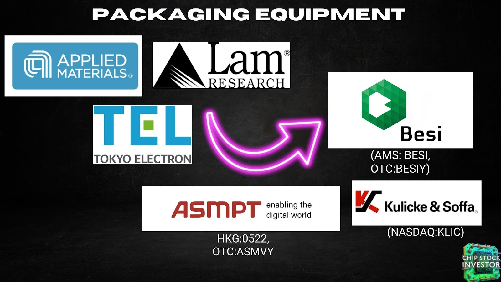
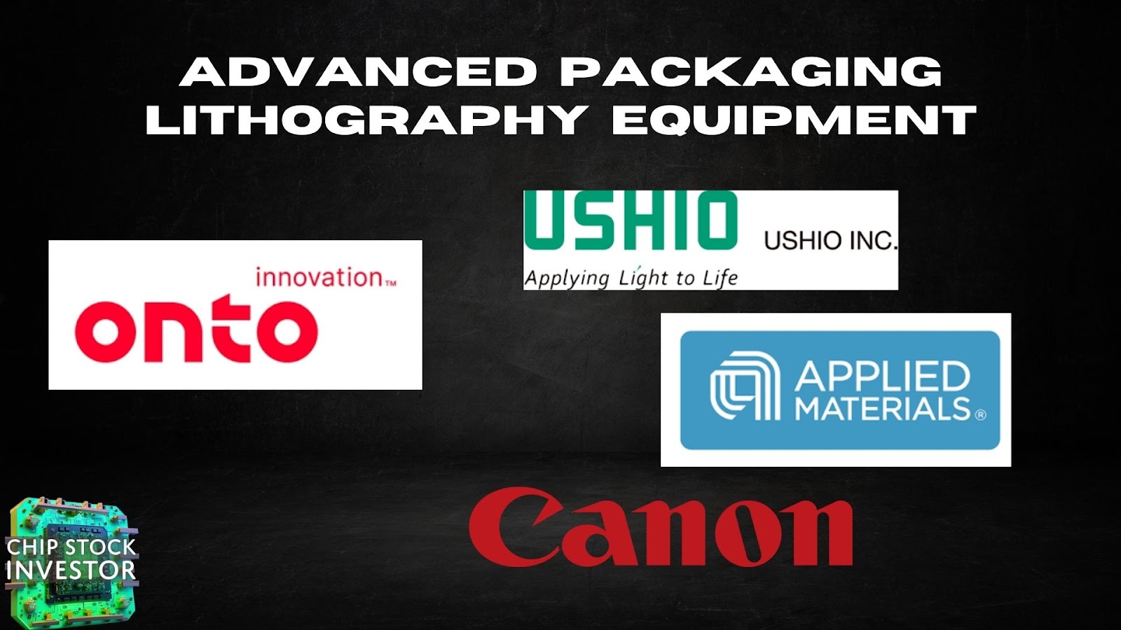
Per usual, when we think about the development of new semiconductor technologies, we here at CSI default to the manufacturing equipment providers. Applied Materials is the leader in advanced packaging equipment, and boasts capabilities in advanced substrates.
Besides Applied Materials, there are some other players in advanced packaging that could roll out some solutions for FOPLP, if it indeed seems it will take off within the next few years.
Investors in South Korea are also familiar with SK Hynix, part of the big SK Group conglomerate. SK Hynix has reportedly been working on a glass panel production facility in the U.S.
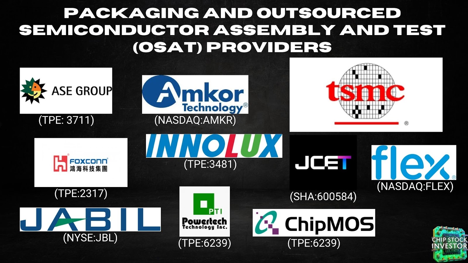
There’s also the third-party packaging and OSAT (outsourced assembly and test) providers. Amkor has significant advanced packaging know-how, including some glass substrates used in limited amounts for some communications applications. But this is a crowded field, and it seems TSMC might be taking the FOPLP opportunity into its own hands with the Innolux factory acquisition.
And of course there’s a different type of lithography involved with developing glass substrates. Applied has partnered with Japan’s Ushio on a digital lithography system for this application. And in the notes that follow from July, we discussed Onto Innovation’s equipment that plays in this potentially emerging field.
Keep an eye on this FOPLP and glass substrate development. This probably won’t be the last time we hear of it.
