
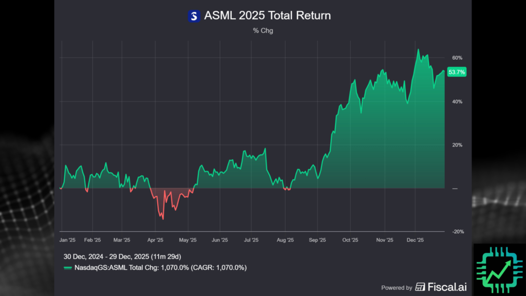
2025 was a wild year for top semiconductor manufacturing equipment provider ASML Holding (ASML). We can divide it in two chapters:
- Through June 2025: ASML’s lithography equipment demand is sluggish, export restrictions and geopolitics between the U.S. and China are hurting, and the stock is still too “expensive” after a selloff from 2024 highs
- Since July 2025: Oh wait, 2026 might be a pretty good year after all, maybe ASML is an “AI stock” darling
The Nasdaq stock listing for ASML, denominated in U.S. dollars, ended up with a more than 50% total return in the last year:
While all the focus is on the current upgrade cycle of newest EUV lithography equipment (see video linked from June 2025 above), what about advanced packaging — a different set of process steps being propelled by new AI performance needs? The following is an excerpt from a write-up we provided our Semi Insider subscribers in October 2025.
What is advanced packaging, and what’s it to ASML?
In mid-2024, we did a series of articles explaining various advanced packaging steps in semiconductor manufacturing — so-called “back-end” processes that gobble up far less in annual capital expenses versus the intensive wafer-level “front-end” development processes. Wafer fab equipment spend is expected to be around $116 billion in 2025, versus about $6 billion for packaging equipment sales, according to latest estimates from Semi.org.
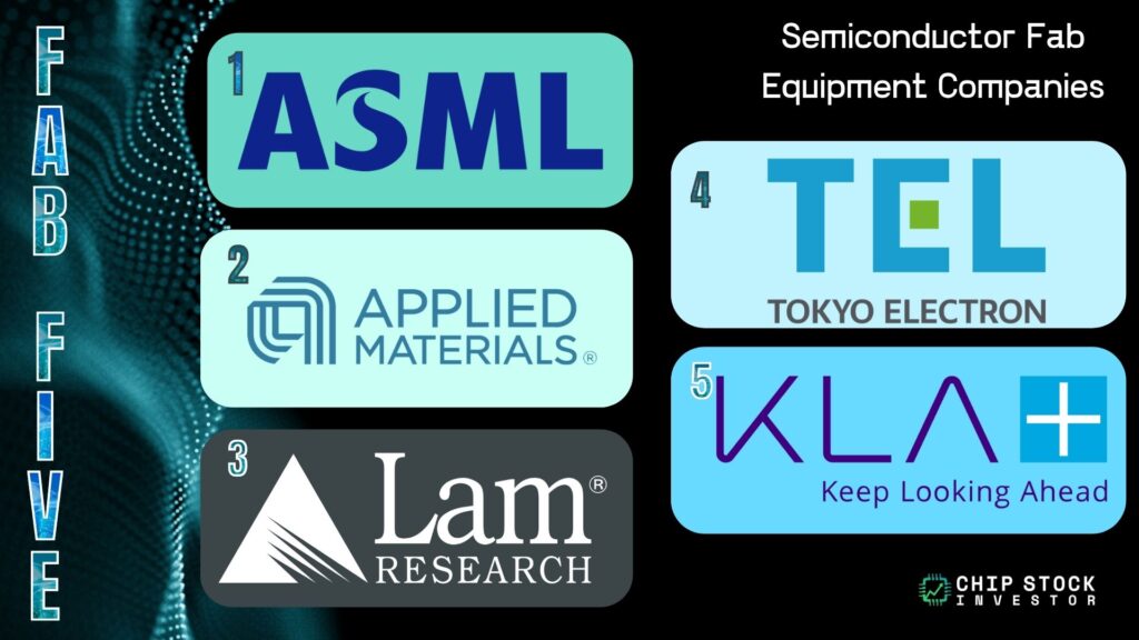
But with wafer-level development scale-down of feature size losing some steam, and cost-per-transistor flying high, the next low-hanging-fruit is packaging processes. This is a market getting lots of attention in the AI era, and an area of the market ASML hasn’t really participated in (the other four of the “Fab 5” have been involved in packaging, though).
Until now. During the Q3 2025 earnings update, ASML management said it shipped its first lithography system used in advanced packaging. There are implications galore, for ASML, and its fab equipment peers alike.
Lithography’s place in advanced packaging
Much like the development steps that are repeated numerous times to create microscopic transistors and other structures on a silicon wafer’s surface — deposition, lithography, etch, clean — advanced packaging actually utilizes the same processes. Lithography is included in these repeatable development steps for packaging.
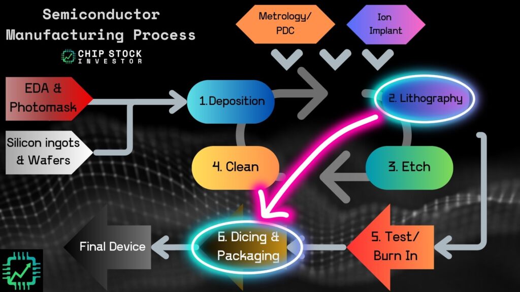
One big difference, though, is that packaging lithography does not require near the same level of technological advancement. Feature sizes in wafer-level and substrate packages are nowhere near the single-digit nanometer (nm) scale of front-end development (transistor and gate scaling). Thus, older lithography equipment tech — ancient by standards of the most advanced EUV systems ASML is selling today — is perfectly capable of handling packaging processes.
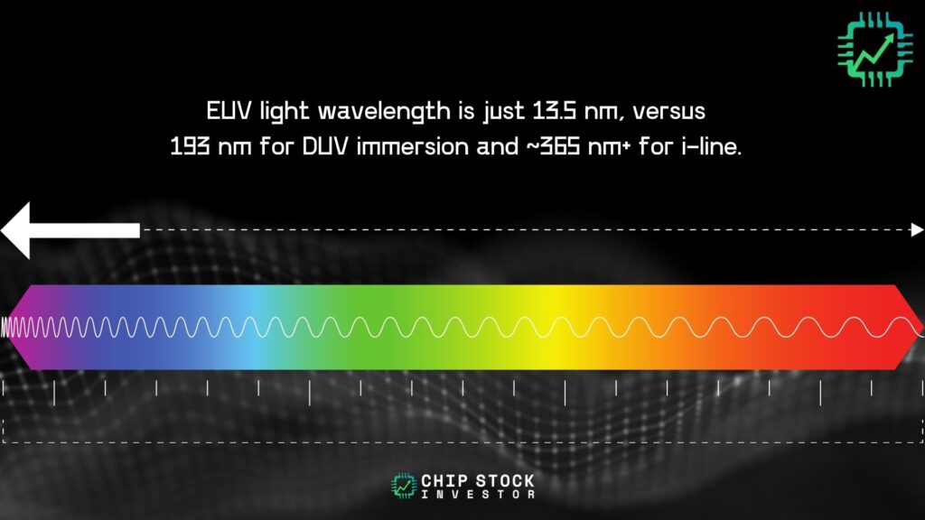
For those of you that have been around this litho business for a long time, it’s time to get reacquainted with “i-line” lithography, which has been around since the 1980s. I-line litho utilizes mercury-based lamps to generate UV light, usually with a wavelength of between 350 nm to 450 nm (compared to 13.5 nm wavelength in EUV, putting EUV close to the x-ray part of the electromagnetic spectrum). https://www.asml.com/en/technology/lithography-principles/light-and-lasers
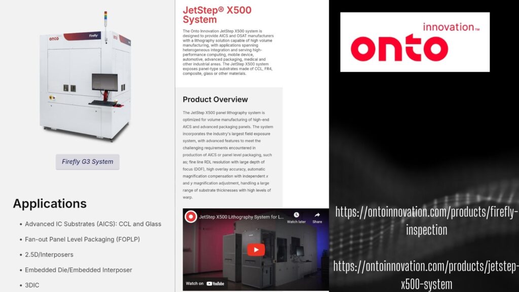
Though the tech is old, that doesn’t mean there aren’t engineering challenges for use of i-line litho for packaging purposes. We’ll address some of these challenges later, but here’s an image from Onto Innovation (ONTO) we discussed over a year ago to help jog your memory (advanced panel substrate litho, including glass).
“Advanced packaging” is too generic a term…
Before getting to ASML’s new i-line machine, we first need to define what advanced packaging is in the first place. Because “advanced packaging” is really quite broad a term.
First, there’s wafer-level packaging, either stitching multiple wafers together before dicing them into “3D stacked” chips (like making a sandwich, and then cutting up the sandwich into bite sizes), or chip-on-wafer where a chip is packaged onto a substrate wafer before being diced up again (putting toppings, like avocado, on top of toast, and then cutting it up into bite sizes). Below is a visual from Taiwan Semiconductor Manufacturing (TSM) illustrating this in generic terms.
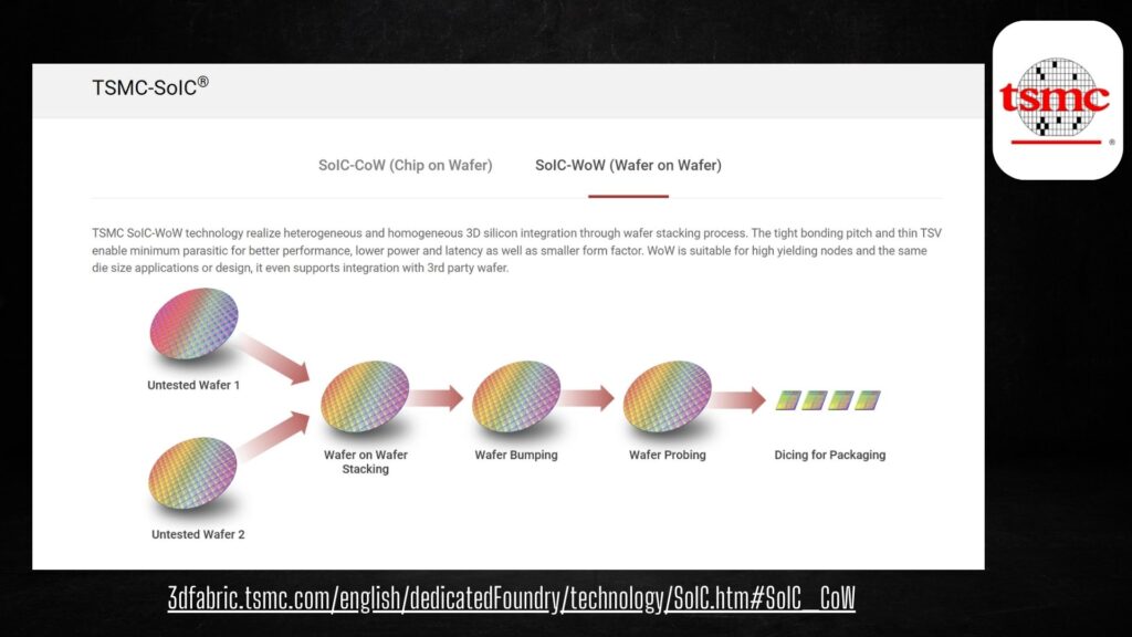
These package methods — be it wafer on wafer, or chip on wafer — can get complex these days with multiple layers using one or both methods shown above. Here are some more TSMC visuals illustrating chips (singles, side-by-side doubles, or even 3D stacked chips) getting packaged on top of a final low-level substrate.

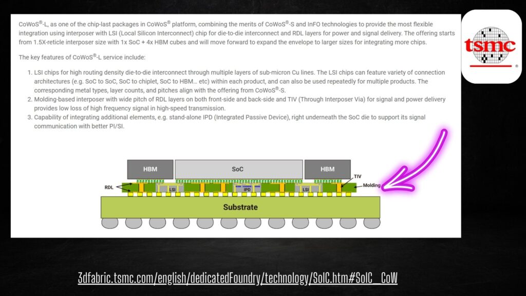
The point of all this, regardless of the layer (chip, interposer package, or substrate), is that lithography is needed to “print” patterns. Sometimes its into wafers and chips to create copper through-silicon-via pillars to interconnect 3D stacked chips (high-bandwidth memory, for one), or into the interposer to create copper interconnects for the side-by-side chips, or into the substrate itself for “powerline” routing to the interposer and chips that are packaged on top.
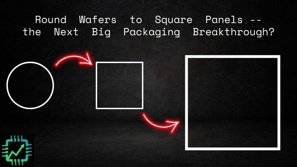
As for these lower level substrates, this is where novel materials like aforementioned glass (our update last year on Onto, Intel (INTC), and TSMC) are being developed. The panels are getting bigger, and changing shape from a round wafer to a square.
Where does ASML fit into the fast-developing packaging landscape?
When discussing advanced packaging, we’re often discussing the companies that help with etch and deposition of TSVs (like Lam Research), or the companies that attach or bond chips-to-chip, chips-to-wafers, or wafers-to-wafers (Applied Materials and their partnership/equity stake in BE Semiconductor).
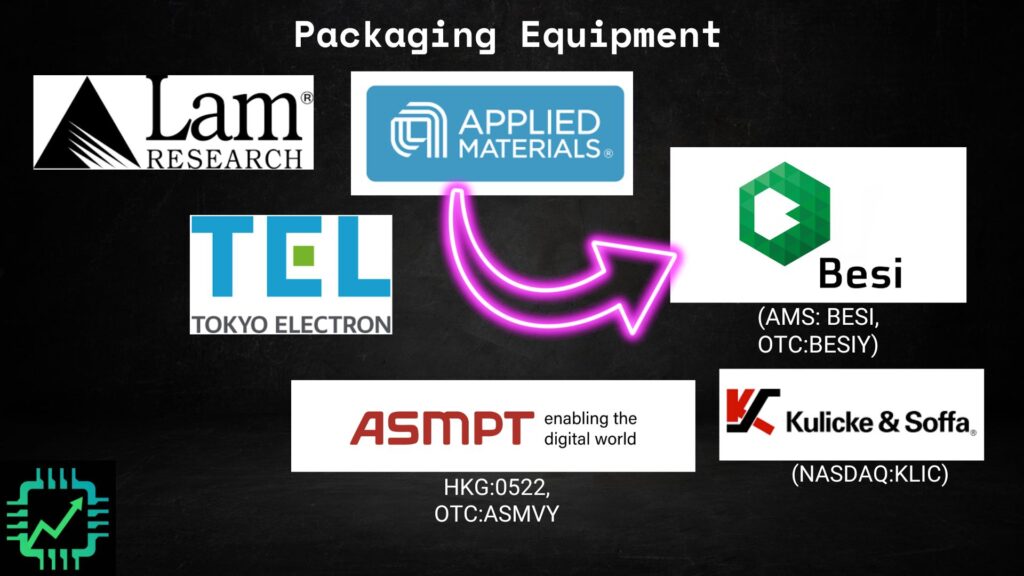
But what about the litho companies involved in printing powerline and interconnect line shapes for the packaging processes? Here they are:

- Applied Materials, which has a development agreement with Japan-based Ushio (6925), not dissimilar from their R&D partnership with BE Semi.
- Onto Innovation mentioned already, developing advanced substrate litho tools, a result of the merger between Nanometrics and Rudolph Technologies — the latter of which had the litho tech.
- Veeco Instruments (VECO), which acquired litho tool tech by way of Ultratech in 2017, and now Veeco is getting acquired by Axcelis Technologies (ACLS).
- Japan-based camera and lens specialists turned industrial conglomerates Canon (7751) and Nikon (7731), as well as small fab and medical equipment company JEOL (6951) also from Japan.
- Jumping to Europe, there’s SUSS MicroTec (SMHN) from Germany, and privately-owned EV Group in Austria.
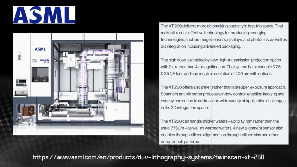
ASML is the newcomer on this list in packaging lithography. Below is the snapshot of the i-line tool shipment from the Q3 2025 earnings release, and some comments from CEO Chistophe Fouquet on the earnings call:
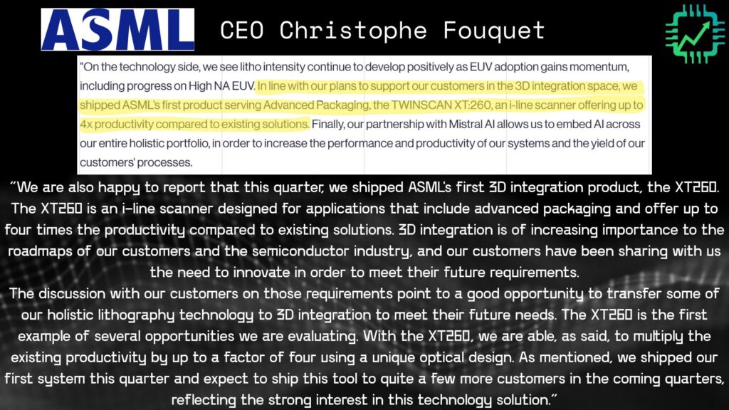
“We are also happy to report that this quarter, we shipped ASML’s first 3D integration product, the XT:260. The XT:260 is an i-line scanner designed for applications that include advanced packaging and offer up to four times the productivity compared to existing solutions. 3D integration is of increasing importance to the roadmaps of our customers and the semiconductor industry, and our customers have been sharing with us the need to innovate in order to meet their future requirements.
“The discussion with our customers on those requirements point to a good opportunity to transfer some of our holistic lithography technology to 3D integration to meet their future needs. The XT:260 is the first example of several opportunities we are evaluating. With the XT:260, we are able, as said, to multiply the existing productivity by up to a factor of four using a unique optical design. As mentioned, we shipped our first system this quarter and expect to ship this tool to quite a few more customers in the coming quarters, reflecting the strong interest in this technology solution.”
The first XT:260 customer is using the machine for 3D integration (vertically-stacked chips), which could mean this is one of the HBM makers. Perhaps new HBM leader SK hynix? Perhaps so…
What is ASML’s new innovation in packaging litho?
If i-line litho has been around for decades, what exactly is the innovation ASML is bringing to the table that customers can’t get elsewhere? After all, why not just use super awesome EUV tech and all its greatness?
Well, at several hundred million euro each, an EUV machine would be overkill in the extreme for current advanced packaging techniques. So an i-line, with some modern updates, are perfectly sufficient.
For one, ASML has been working for some time on challenges arising from wafer warpage with its i-line Twinscan XT lineup. Even tiny dimensional changes arising from the most imperceptible of wafer warpage can mean mis-alignment of TSVs and other features when it comes time to start stacking chips on top of each other. The other is gradual semi manufacturers gradually switching from smaller 200mm diameter to larger and better-yielding 300mm diameter wafers. It sounds like a simple task to just make bigger wafers, but backward and forward compatibility between 200mm and 300mm equipment doesn’t come easily. The Twinscan XT equipment teams at ASML been working on these challenges.
As for the new Twinscan XT:260 specifically, ASML created a custom optics system to help increase resolution of features. And the XT:260 also features a “scanner,” instead of the more commonplace “stepper” available from a lot of competitors.
A “scanner” system is a method of gradually exposing an entire wafer to the patterned UV light (sort of like how your office photocopier works); versus the older litho industry “stepper” method that exposes a small part of the pattern onto the wafer at a time before moving to the next section. A scanner generally can complete more wafers, making it ideal for modern high-volume production.
ASML has a new growth lever ready to go for 2026. Will this new advanced packaging litho tool move the needle for ASML? All on its own, probably not. But things are moving quickly in the semi industry due to demands from AI, and ASML is getting itself in better position to address those needs.
See you over on Semi Insider for more on ASML, advanced packaging, and an expected banner year for fab equipment sales in 2026.
