The following post was provided to Semi Insiders in March 2025, and was the basis for the video linked above. It’s been a bumpy road, but the recent advance of wafer fab equipment (WFE) providers was always imminent given the coming roadmap of semiconductor innovation. And the road ahead for more innovation is long, and winding…
The future of chip technology – where is it being developed?
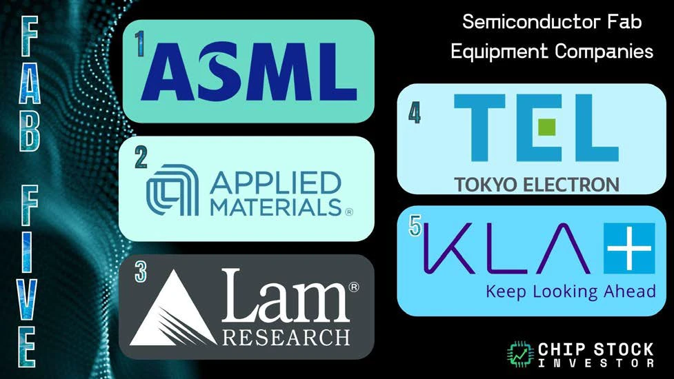
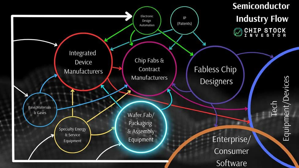
Whenever we’re talking about research and development (R&D) of semiconductors, we like to default to the critical chokepoint in the industry where actual manufacturing process tech resides: Wafer fab, testing, and chip packaging equipment companies. Specifically within this sub-industry is the “Fab 5,” which account for ~70% of all the market cap and revenue of this part of the chip supply chain.

The Fab 5 are as follows, in order of size (both by market cap and total sales):
- ASML Holding (ASML), a type of “monopoly” on the most advanced lithography equipment.
- Applied Materials (AMAT), a generalist that supplies a lot of deposition equipment, as well as manufacturing process equipment for virtually every other step in chipmaking.
- Lam Research (LRCX), another generalist that historically supplies a lot of equipment to memory chip manufacturers.
- Tokyo Electron (TOELY), the smallest generalist in the Fab 5, but also a supplier of all sorts of manufacturing process equipment except for lithography.
- KLA Corp (KLAC), a specialist in metrology (the science of measuring stuff) and process diagnostic and control equipment.
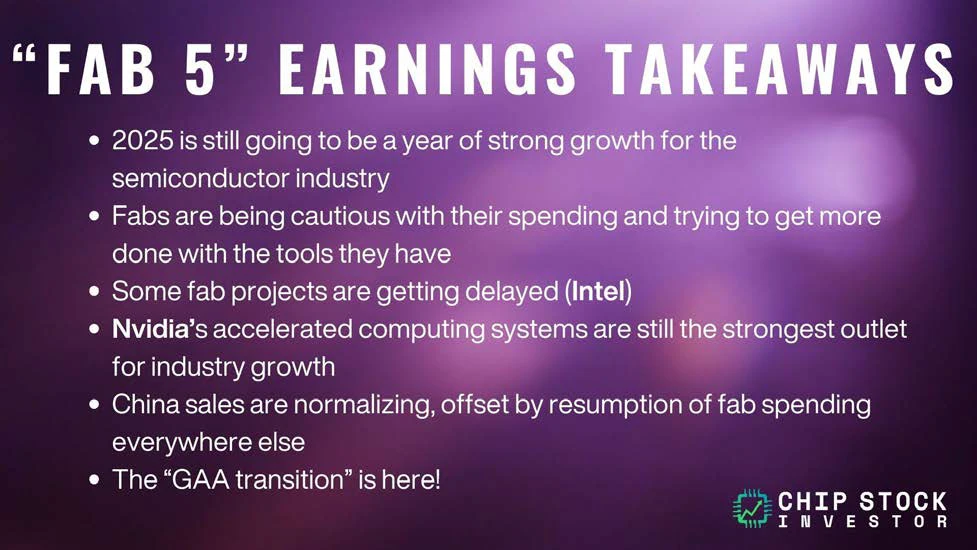
Q4 earnings season is over, and we got some insight into 2025. We’re optimistic for the Fab 5 and other participants in the greater wafer fab equipment sub-industry.But one big question did arise on earnings calls and other investor updates from these companies: What the heck is GAA? And why does it matter?
Why GAA matters
Let’s first start with the WHY. GAA matters because the “GAA manufacturing transition” is what the Fab 5 have been saying will drive the “U-shaped recovery” in industry revenue later in 2025.
Let’s start with some commentary from ASML’s investor day update from back in November 2024 (sorry, we’ve been sitting on these notes for too long!).
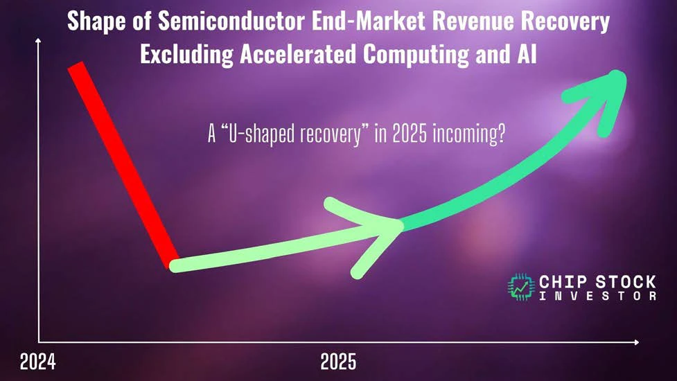
Data center servers have become the largest end market for chips, and is hoped AI servers will be the primary driver of industry growth for the next 5 years. Aka, AI is the new secular growth trend. See the middle tile in the slide below from ASML:
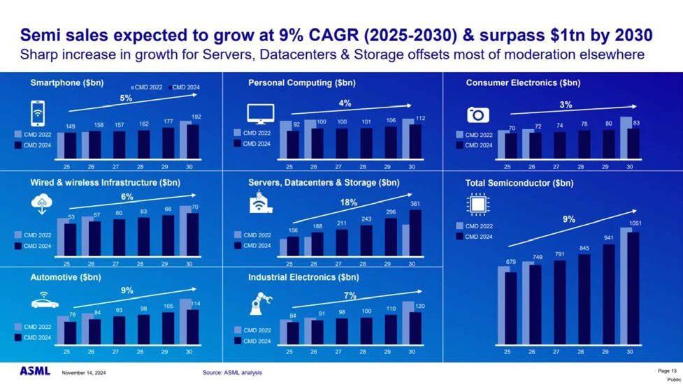
We discussed this briefly a few months ago following ASML’s investor day (ASML Just Confirmed This Critical Data Point Investors Need to Know About), but despite this secular growth trend from data centers and AI, the path to growth for the Fab 5 is not going to go up in a straight line. 2024 was proof of that.
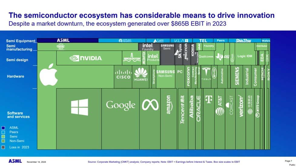
However, for patient investors, there is a massive amount of money being spent on R&D for new types of logic chips right now. A couple of years ago, investors may have balked at the below chart and said most of the companies listed on it aren’t chip designers. But today, most now understand the level of custom chip design work that is going on across what we traditionally consider the tech industry, as well as communications, auto/industrial, and more. Chips aren’t the new oil, data is, but chips are modern infrastructure that every business needs to be concerned with in the 21st century. And these companies are perpetuating a virtuous cycle of chip technology advancement… the latest of which is this thing called GAA.
Note how ASML has itself and its peers listed along the top of the chart. There’s a reason why…
A bit of chip manufacturing background before defining GAA
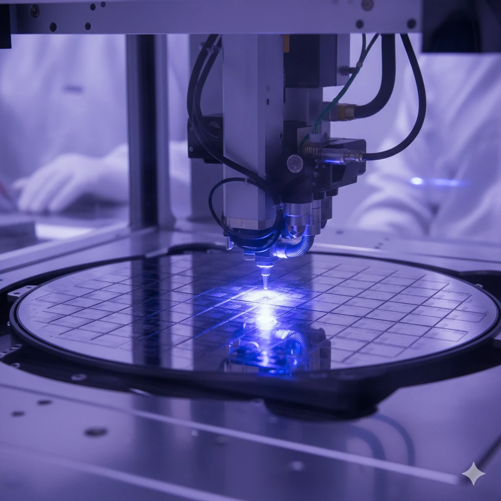
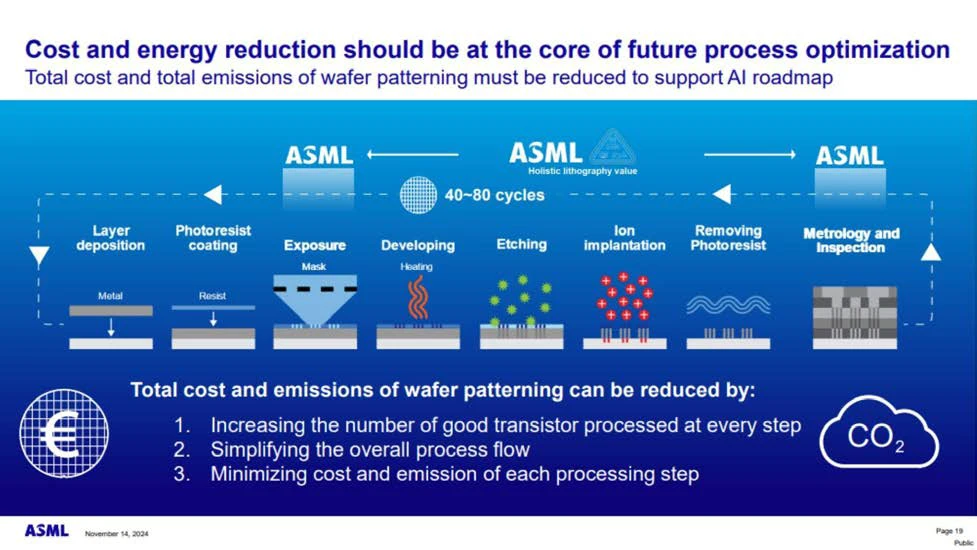
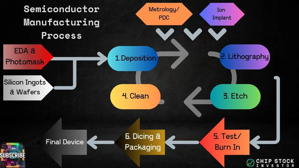
Let’s quickly review what the Fab 5 does. In this next segment, we will focus on the four primary manufacturing steps in the middle of our below chart. These four steps create a repeatable process in crafting microscopic features on silicon wafers: Deposition, lithography, etch, and clean/process.

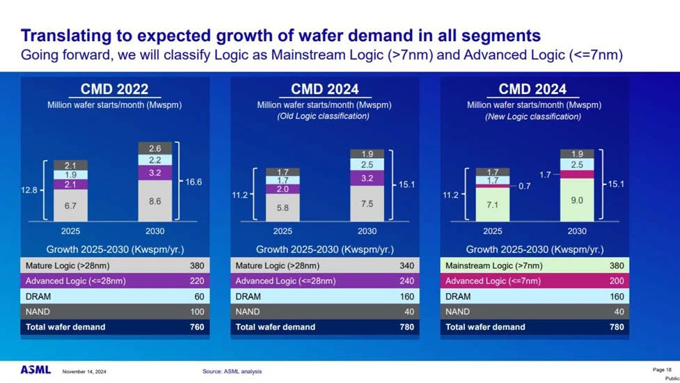
Since we’re discussing ASML’s last investor day update, let’s actually start with step number two: Lithography. Lithography is the process that uses ultraviolet (UV) light to “print” tiny patterns onto silicon wafers. Thanks to R&D efforts across the whole semi industry, ASML believes it has a long runway of growth for its lithography machines through the end of the 2020s. Advanced logic (which it just re-defined as 7-nanometer and smaller manufacturing technology, see below chart with the new advanced logic segment now in pink) is especially expected to contribute to this rising demand.
ASML is currently in the early stages of selling its extreme UV (EUV) high-NA machine (0.55 numerical aperture), shown in the bottom right part of the timeline below. Sometime at the end of this decade or the beginning of the next, there will be another EUV machine with a 0.75 numerical aperture that will further increase the resolution of the tiny printed designs.
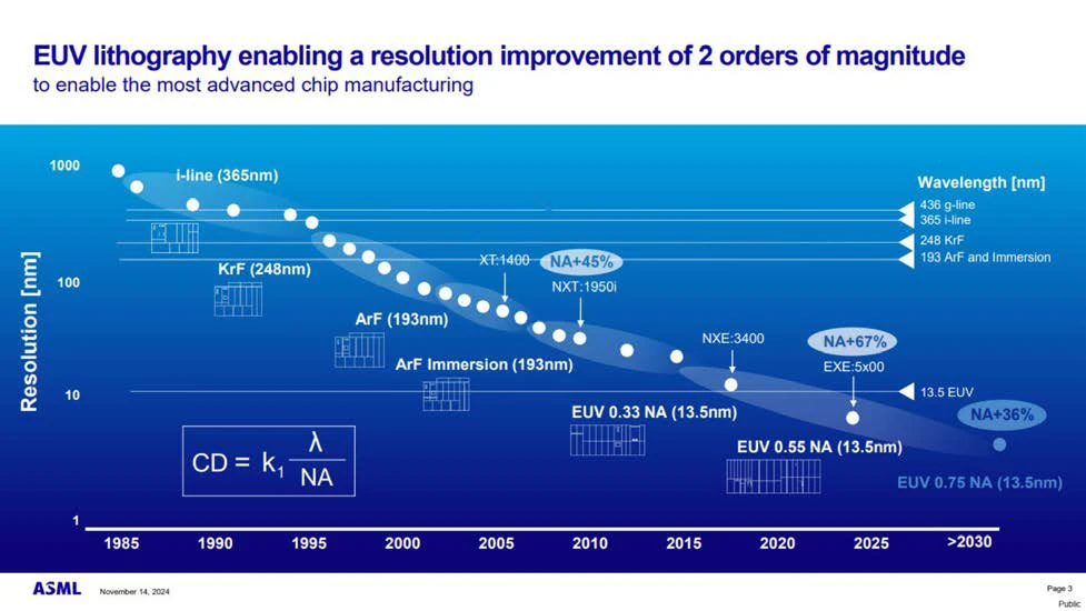
These high-NA EUV machines are expensive, with the cost steadily rising with each new advance in ASML’s equipment. The new high-NA machines (the “EXE” models) cost somewhere in the range of a few hundred million euro each.
If you want to make financial visuals like the above charts, and get 15% off, visit our special link: Fiscal.ai/csi!
Why are chip manufacturers spending that kind of money? And why does ASML have confidence they’ll keep buying at ever-higher prices? The reason for that, as explained in November, is we actually have about 15 years of visibility into one of the most important features of those printed circuit features.
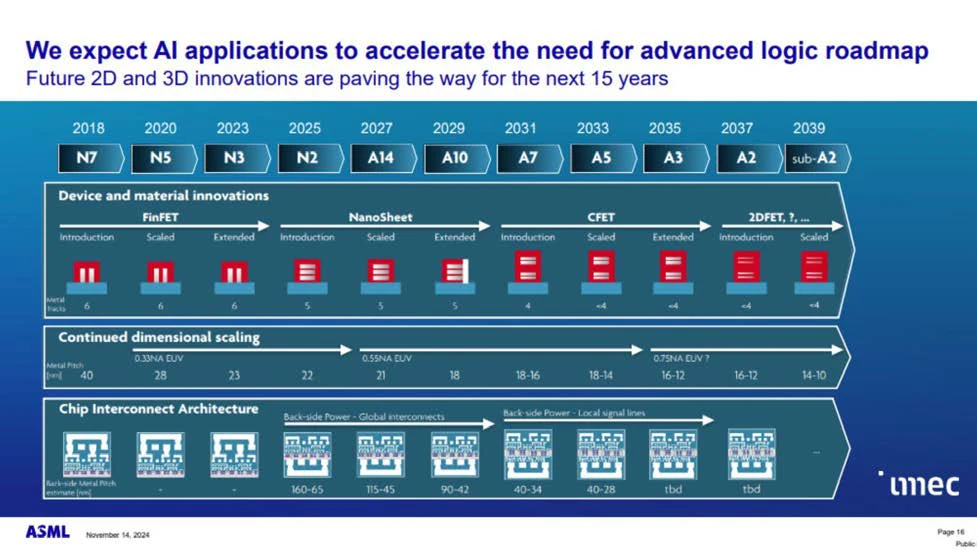
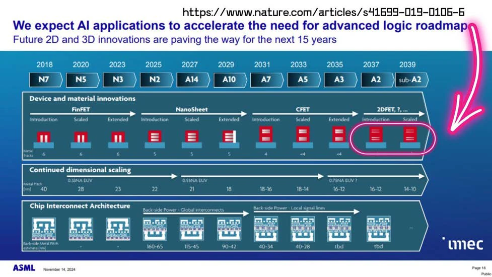
On the top row of the next chart, ASML has listed the general manufacturing process nomenclature. The last two years, TSMC has been rolling out N3 (3-nanometer) manufacturing process for its customers. Just a reminder the “N3” and so on no longer refers to the actual chip smallest-feature size, but rather to old feature size performance equivalents using logic chip architectures of the past. We will get to this in just a moment. But at N2, shown as beginning this year in 2025, there’s a new “device and material innovation” that takes over from “FinFET” of the past (shown just below row one).
What is this “NanoSheet” thing, and what does it have to do with the GAA transition?
Just spit it out! What is GAA?!?
In 2025, in the first row, N2 is listed. This is the beginning of what is being called the NanoSheet (or nanowire, or ribbonFET technology, depending on who you ask). For our purposes here, let’s just call it GAA, or gate-all-around logic chip architecture.
The following is a simplified picture of the design of the transistor. The transistor is a type of electron gate, the microscopic device in logic chips that are responsible for the 1s and 0s that form the foundation of software and govern how computers operate.
For decades under Moore’s Law, we were primarily dealing with the planarFET (FET = field effect transistor). Imagine the green-colored portion on the left hand side of the red block (the gate) is the source of the electrical signal, and the green portion on the right is the drain.
That red block, or gate, uses an electric field to control the flow of electrons from the source to the drain (thus the “field effect” in the “FET” acronym). When that electric field gate is closed, the flow of electrons stop (a 0), and when the electric field is “open” the electrons flow through (a 1).
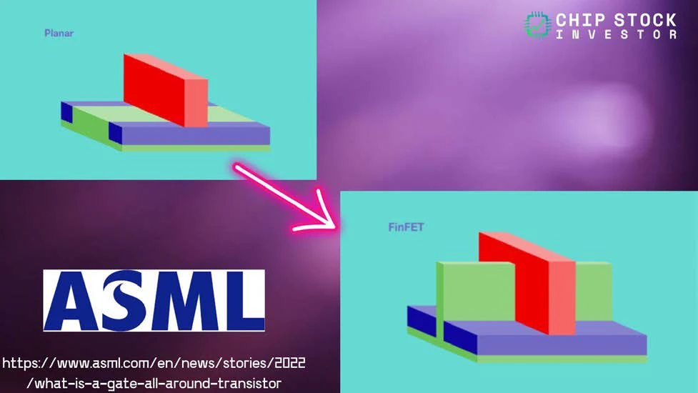
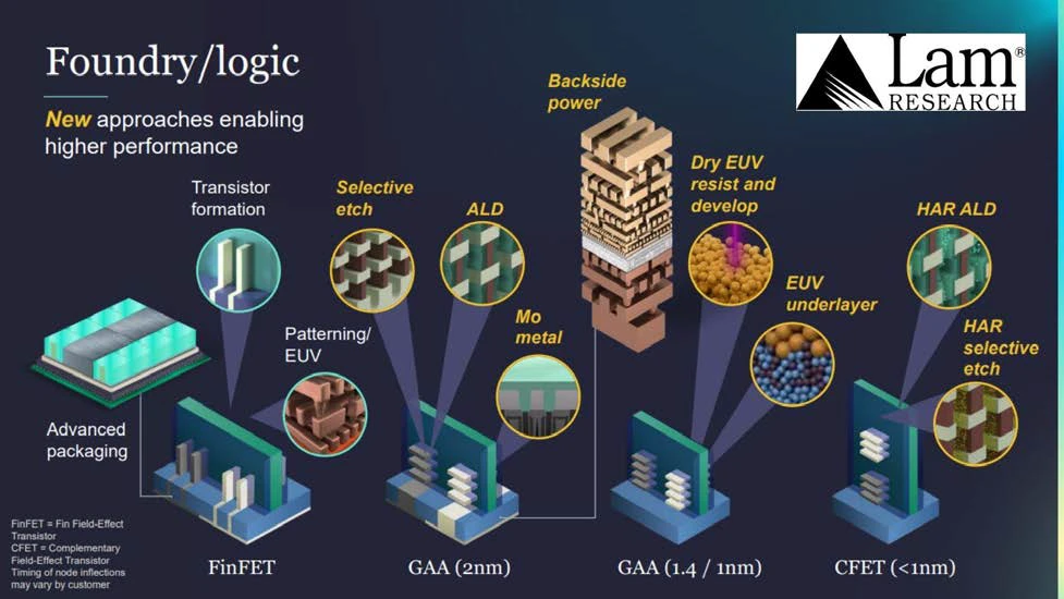
However, as these little transistor devices shrunk in size over the decades, the green channels could no longer be controlled by the small electric field created by the red block. And so to compensate, these channels were raised to make contact with the gate, like a shark fin poking out from the surface of the water – thus the name “finFET.” This finFET architecture was first released in 2011 by Intel, then a couple of years later by Samsung and TSMC.
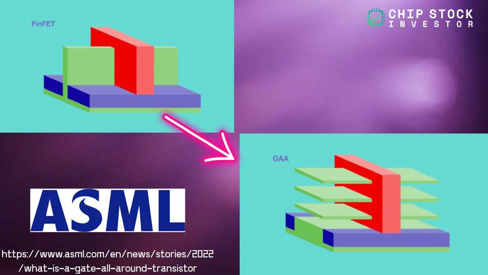
But at N3 and smaller, the power of the finFET is starting to reach its limit too. And so we are making the transition to a new architecture called gate-all-around, or GAA. As we enter the N2 and “smaller” era, logic chips manufactured at scale first by TSMC, and later at Intel and Samsung, will begin offering GAA architecture logic chips as well. There are some great videos on the manufacturing steps involved in making these tiny GAA features from Applied, ASML, Lam and others. We will also link a video from Asianometry on this process. https://youtu.be/5RPFfPtgw7g?si=SVahQVfcYFcBGdTB
https://www.asml.com/en/news/stories/2022/what-is-a-gate-all-around-transistor
https://www.imec-int.com/en/articles/imec-puts-complementary-fet-cfet-logic-technology-roadmap
For the next two years, the most advanced logic chips (GPUs and CPUs) will be making this transition from the older finFET to GAA. Notice the green fin has now been replaced with horizontal sources and drains that make full contact with the red block (the gate), which can more precisely control the flow of electrons thanks to this architecture. The shape of these horizontal sources and drains is where the “nanosheet” or “ribbbonFET” names come from, as the devices are made by alternating layers of silicon and silicon-germanium, the latter of which is etched away. It’s ASML’s lithography equipment that plays a key role in making these microscopic features possible in the first place (of course with a big helping hand, and R&D collaboration, from peers in the Fab 5 and wafer fab sub-industry).
The next 15 years of logic chip R&D
But we called this segment the next 15 years of logic chip R&D. So what about after the next two years of GAA transition? What comes next?
As we get closer to 2030, we will likely start hearing a lot more about the CFET, or complementary FET. We pulled this side view schematic of the logic gate and the little side view of the FETs, from EDA software leader Synopsys. https://www.synopsys.com/blogs/chip-design/what-are-gate-all-around-gaa-transistors.html
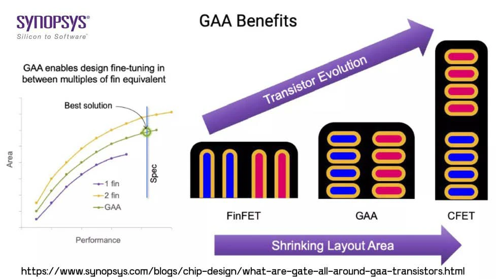
The blue part of the design is called an N-FET (the source), and the red is the P-FET (the drain). The N-FET is where the electrons flow from and the red (P-FET) is where they land after they cross the gate. In both GAA architecture and FinFET before it, these N-FETs and P-FETs are placed side by side. CFET architecture, though, could stack these sources and drains on top of each other to save space and further increase logic chip performance and power consumption.
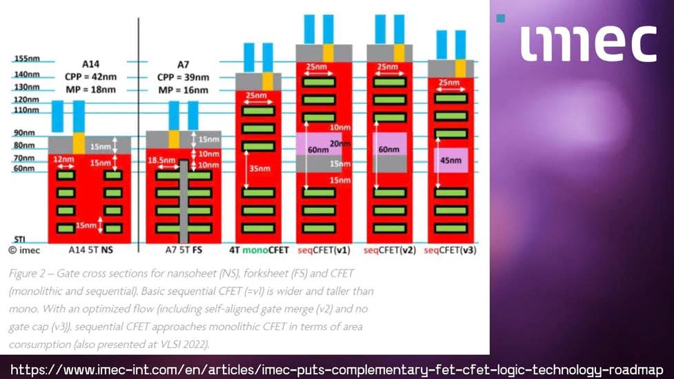
Here’s a similar schematic from IMEC, which shows how this architecture R&D could play out. GAA is shown on the far left, and there is an intermediary architecture between GAA and CFET, called a “forksheet.” The name forksheet derives from the gray wall, like a fork stabbed through the layers, separating the N- and P-FETs from each other. https://www.imec-int.com/en/articles/imec-puts-complementary-fet-cfet-logic-technology-roadmap
Beyond forksheet, technologies are currently being researched that would develop the N- and P-FETs separately and perhaps use a type of wafer bonding to stack them on top of each other. Or a sequential process could be used that builds these FETs up to create a new type wholly integrated 3D transistor.
What does this mean for ASML and the Fab 5? The GAA transition is creating a new inflection point for cyclical growth expected to kick in the second half of 2025. New processes means new equipment needs to be sold. The new GAA architecture can be perfected over time to increase further adoption of the manufacturing process later on, which further broadens wafer fab equipment sales.
Note this ASML slide has just taken the middle four cycles, deposition, litho, etch, ion implantation, metrology, and clean/process and put them in a straight line. This chart corresponds with our primary process cycle of deposition-litho-etch-clean.
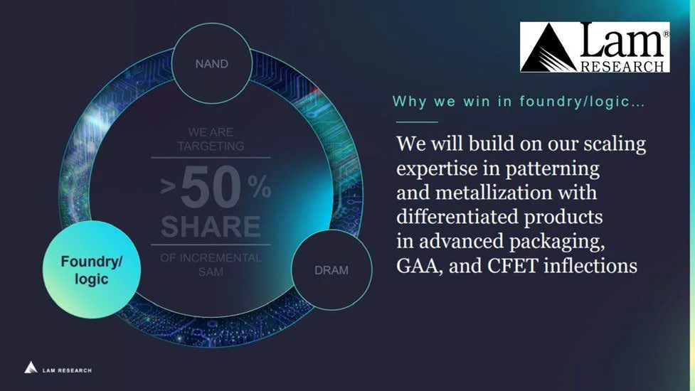
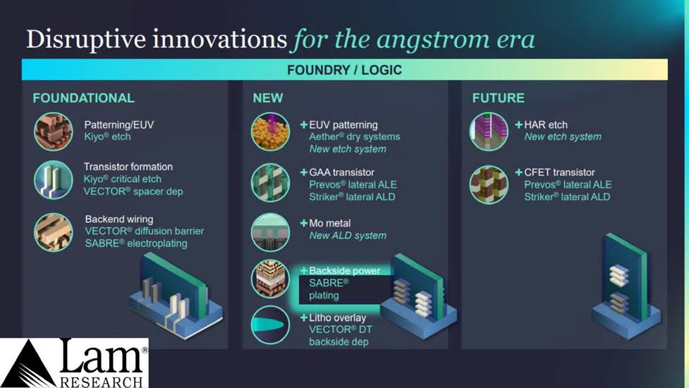
Lam Research joins the CFET party early?
Lam was the other company of the Fab 5 to mention not only the GAA transition, but also the coming CFET transition, at their investor day in February 2025. Lam also has a blog article explaining CFETs, and the R&D needed to pull off stacking the N-FETs and P-FETs on top of each other. https://newsroom.lamresearch.com/understanding-cfets-transistor-architecture
This GAA transition and future CFET architecture transition require new types of equipment for the manufacturing processes involved. For example, advanced deposition methods like ALD (or atomic layer deposition, an equipment type that ASM International specializes in) and selective etch using plasma (ionized matter) are going to be required for GAA. More precise versions of both of these deposition and etch processes used for GAA will be needed for CFET in approximately 5 years, according to Lam.
This is why ASML has been talking up its high-NA EUV machines, and Lam Research its various new product families to support GAA logic chip architecture. This isn’t going to be a full-on logic chip manufacturing revolution. GAA, and later forksheet and CFET, builds on past advancements. But the introduction of these new processes is what drives the cycles of growth for the Fab 5, since they are the ones largely responsible for developing the specific manufacturing technology processes later utilized by the advanced logic chipmakers TSMC, Intel, and Samsung. (Note, there are 10 “Angstroms” in a nanometer, so beyond N2, chip manufacturers may switch to naming their process nodes by the size of Angstrom equivalent transistors.)
Chip technology as we approach 2040?
GAA, forksheet, and CFET architecture could get us all the way out to year 2035, give or take a few years. (Our guess is to give it an extra three years. Let’s face it, this equipment is super expensive, and chip manufacturers like to extend the use of their current manufacturing line for as long as they possibly can.)
What about the second half of the 2030s? What is the 2D-FET? We have listed a study published in Nature on this, as the evolution of the CFET in the 2030s could get really interesting as new materials, other than silicon, are being experimented with to further drive the performance of the transistor. https://www.nature.com/articles/s41699-019-0106-6
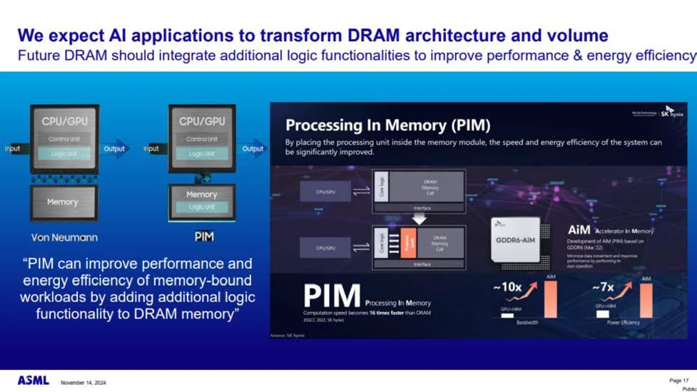
For this discussion, we have only been talking about logic chip architecture. There is a lot going on in memory as well, especially in HBM (high-bandwidth memory) DRAM. There is plenty of talk about the networking bottleneck between logic and memory chips in data center AI servers. We think this is less of a bottleneck than is sometimes described, and a type of merging of logic and memory architectures is being developed by bringing more of the logic functionality directly to the HBM memory. But that is a discussion for another time. First, we need to discuss the current landscape of the memory chip IDMs. The next segment of our Semiconductor Industry Flow will tackle the memory chip makers, and how the groundwork for commoditization of HBM has already been laid for this ultra-advanced memory type by companies like Nvidia and Broadcom.
Investing in 15 years of logic chip R&D
So how do you invest in the next 15 years of logic chip architecture technology development? A basket of holdings in the Fab 5, though highly cyclical, is a great place to start. These companies are peers, and they do compete with each other – especially during big technology inflection points like GAA (note Lam talking about taking market share in the new processes involved in GAA on previous slides).
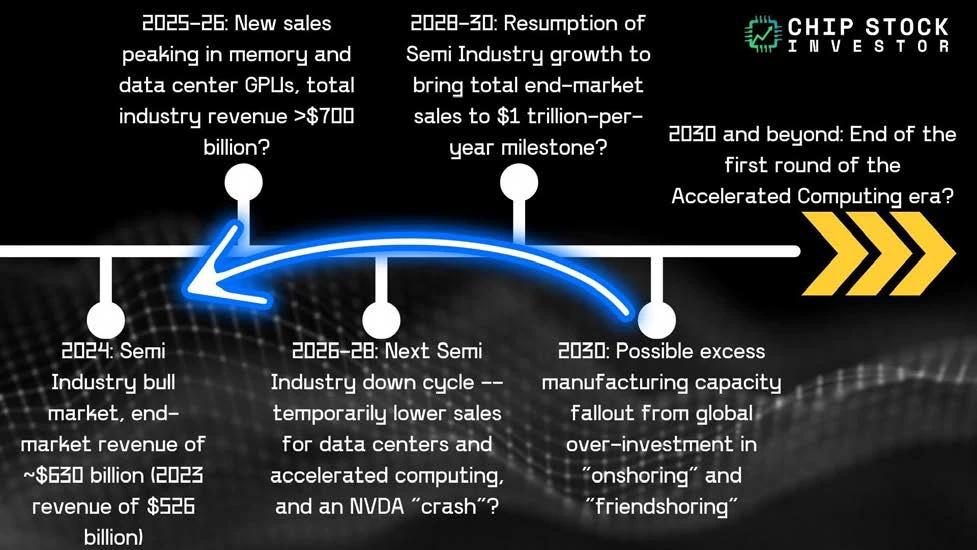
Mind the cyclicality inherent in investing in these industrial equipment providers. We’ve been discussing the risk with excess chip manufacturing capacity since we started this channel over two years ago. But a sizable part of this over-capacity risk struck hard in 2024, especially among “mature” manufacturing node providers – especially those that participate in the auto/industrial/power segments of the chip end market. This cycle is what hit the Fab 5 stocks in the last year.
However, taken collectively as a type of “single position,” the Fab 5 is a powerful oligarchy, one that could continue to dominate the wafer fab/packaging sub-industry for decades. We own a basket of the Fab 5, and some of the smaller players like Onto Innovation (ONTO). We also recently bought small starter positions (less than 0.5% of our portfolio in total) in Nova Ltd. (NVMI) and Camtek (CAMT).

One Response