
The last couple of years, HBM (high-bandwidth memory) has been all the rage. (See our write-up on HBM here.) HBM was one of the innovations that has helped new AI (like LLMs) get trained in an increasingly efficient manner.
AI inference is the next phase of the AI data center build, and new memory architectures are needed. Sandisk (SNDK) has been hard at work developing HBF, or high-bandwidth flash. This promising new memory technology is one of the reasons for the stock rocketing higher. But what is HBF? And should investors care about it?
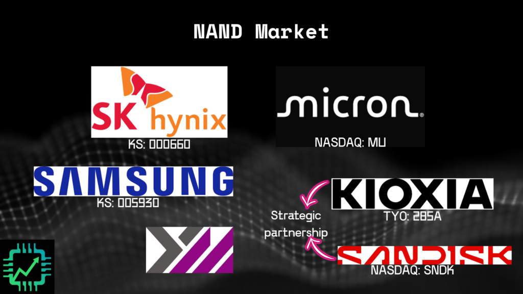
A quick rundown on the NAND flash market
Just as HBM is a type of DRAM (dynamic random access memory) product, so HBF is to NAND (not-and) flash memory. HBF is a new type of NAND flash product. Let’s thus start with an overview of the NAND flash market.
Want to make financial visuals like the one above part of your investing process? Check out Fiscal.ai, and get 15% any paid plan with our special link! fiscal.ai/csi/
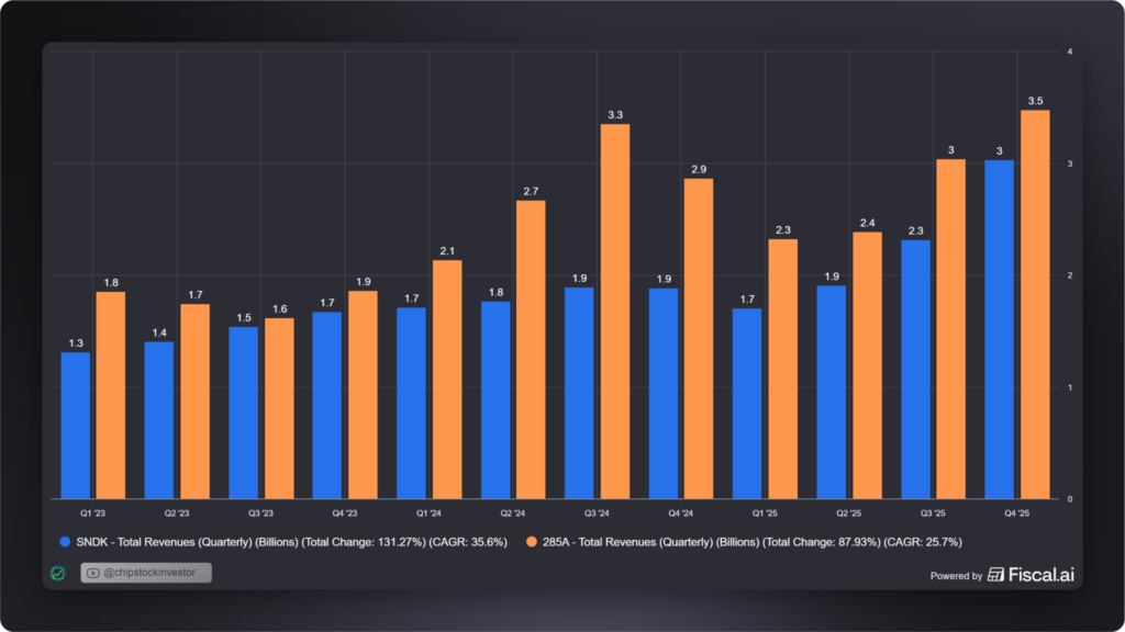
Note: As the 51% owner of the manufacturing joint venture with Sandisk, Kioxia is responsible for operating the NAND flash wafer fabs, but does not provide a specific breakdown of revenues; ie. NAND flash vs. SSD (solid-state drive) storage device sales.
What is NAND flash?
NAND flash is a semiconductor-based non-volatile long-term storage medium. This is as opposed to the older hard-disk drive (HDD) technology, which uses spinning magnetic platters as a long-term storage medium.
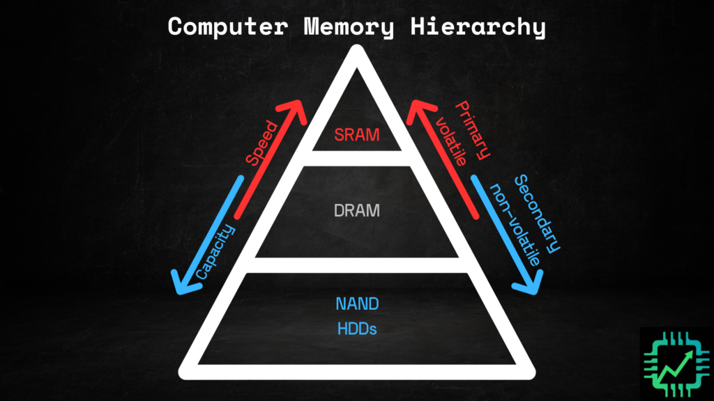
There is a trade-off between storage capacity and bandwidth (the speed at which data can be read or written to the storage device). Higher storage capacity means slower speed. Higher speed means lower storage capacity. NAND flash boasts high-performance speed for long-term storage, but it doesn’t match DRAM (and HBM) in terms of bandwidth.
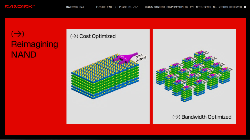
This trade-off, however, is constantly improved in typical semiconductor industry fashion: Shrinking down transistor size (and more recently, improving advanced packaging techniques) lowers computing cost and increases performance. And that’s where HBF comes in.
What is HBF?
HBF aims to take the high-capacity cost-optimized storage advantages of NAND flash, but apply breakthroughs in manufacturing to greatly improve bandwidth speed. The marriage of the two is a memory semiconductor device that looks similar to the now-familiar HBM.
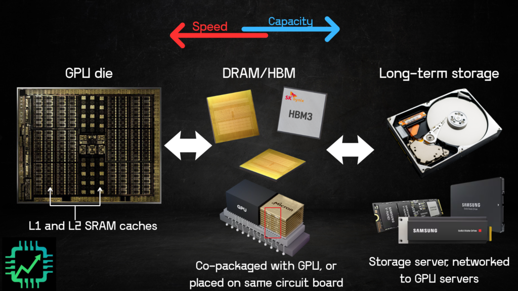
Sandisk, together with its partner Kioxia, are currently sending product samples to customers of their 3D NAND using 9th gen BiCS (bit-cost scalable) manufacturing process. HBF, which will begin sampling to customers the second half of 2026, stacks up to 16 of these BiCS 9 NAND flash wafers together (using Sandisk’s CBA, or CMOS directly Bonded to Array), with a logic controller device at the bottom to handle read-write communications with the co-packaged GPU, CPU, or TPU. The architecture is thus quite similar to that of the DRAM stacking technique to make HBM.
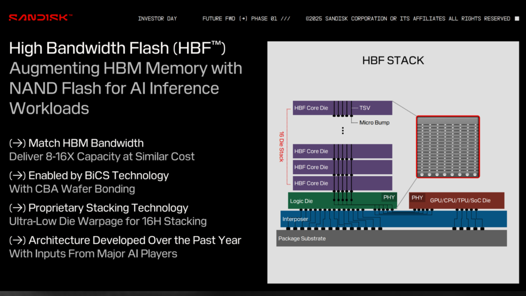
The potential benefit of HBF, though, is exponentially more storage capacity co-packaged next to those GPUs. For AI inference, this could be a significant improvement versus using just high-bandwidth but lower-storage capacity HBM.
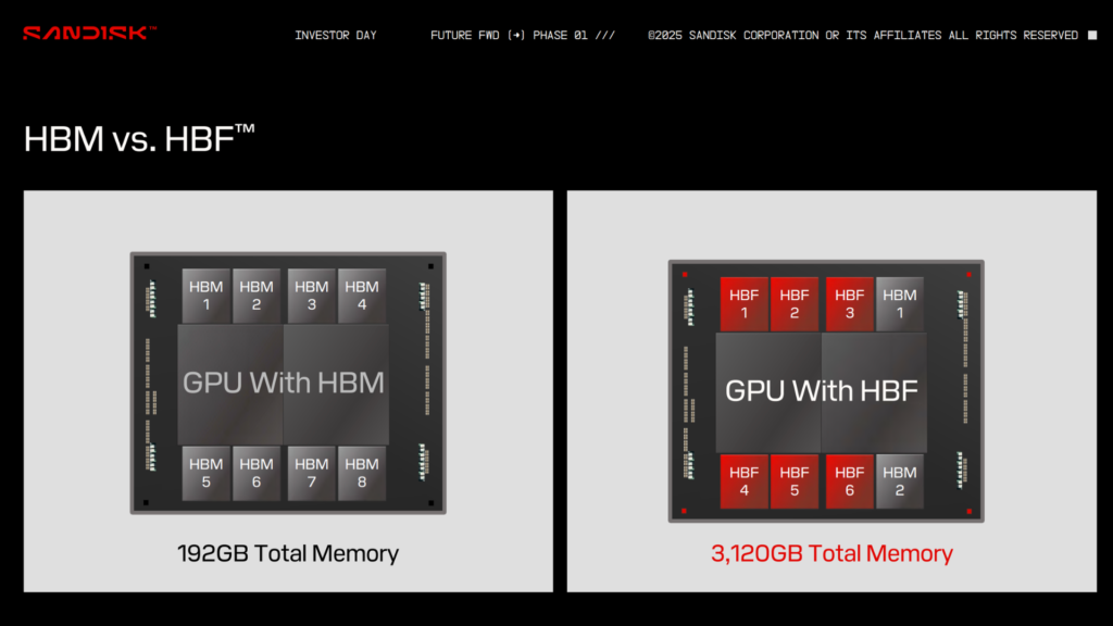
As an important aside, HBF isn’t targeting replacement or competition with HBM. Rather, the hope is HBF will be a new layer in the memory hierarchy, sandwiched between high-capacity NAND flash SSDs/legacy HDDs, and higher-bandwidth DRAM products like HBM.
Should investors care about HBF?
Most certainly, yes. With GPU data center systems (accelerated computing) improving at a far faster pace than memory, the semiconductor world has been working on solutions to bridge the gap. HBF could be one way for that memory capacity-to-bandwidth tradeoff to keep pace with data hungry GPUs.
To help open up HBF to further advancement, Sandisk announced a partnership with SK hynix in 2025 to standardize the technology. Standardization is an important step in the development phase, ensuring that a new product category has interoperability with other semiconductor devices and computing systems and helps pave the way for lower cost mass manufacturing, among other things.
Sandisk and SK hynix officially began standardization work on next-gen HBF in early 2026.
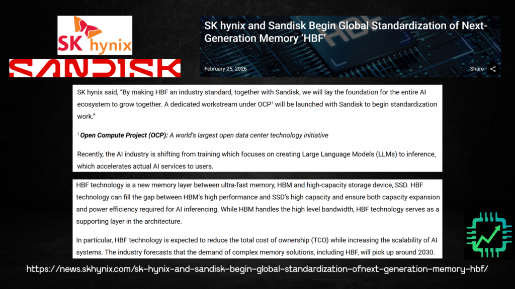
But an important caveat for investors to consider: While early customer samples will begin shipping later this year and into 2027, wider adoption of HBF isn’t expected to pick up pace until late in the 2020s, or “around 2030,” as SK hynix noted in its press release.
Thus, HBF won’t meaningfully contribute to Sandisk/Kioxia’s revenue for some time. At this stage of the AI data center buildout cycle, high-capacity NAND flash is what’s moving the needle as data center operators begin modernizing their long-term storage architecture for the future. And besides NAND flash, HDDs are also still being featured prominently.
And as always, the equipment providers are also involved in the R&D, and will be responsible for developing manufacturing process IP. Suffice to say there’s a long runway of hardware development ahead for these companies, even though their valuations currently sit near the high end of their historical average.
Join us over on Semi Insider and the Chip Stock Investor Research Dashboard for more of the conversation! Get access to all our research, weekly live Q&A sessions, financial data powered by Fiscal.ai, and a growing list of investment tools.

One Response
There was no mention on whether Sandisk’s HBF product development is a major competitive threat to Micron and whether Micron also has an HBF product in development? Thank you.