
Let’s talk about the Netherlands’ other dominant semiconductor fab equipment company (no, not ASML), BE Semiconductor (BESI in Europe, BESIY in U.S.). After listening to the investor day update, we decided this one was worthy of a deeper dive. It’s not new info for those of you that have been following the advanced packaging topic along with us for the last few years, but if you haven’t, let’s get you up to speed.
Below is an excerpt from our Semiconductor Insider deep dive on where BESI is today (as of last report for Q1 2025), and after the investor day.
Note the poor looking revenue results the last few years due to the semi industry downturn — much of BESI’s packaging business is tied to non-AI chips. As a result, the earnings multiples look very high. But let’s not call them “expensive” just yet. There are big changes coming for BESI and the chip packaging market, driven by none other than AI and accelerated computing technology.

We use Fiscal.ai (formerly Finchat) for business-level research and for visualizing financials. Get 15% your own paid plan using our link here!
We first need to do a quick sub-industry intro before we talk about BESI’s Investor Day update.
We’ll start with the Semiconductor Industry Flow. The top half of this flow chart is the chip design part of the supply chain (where software is turned into new invention pf next-gen chips), and there in the middle is the manufacturing layer, especially the IDMs (on the left) and the contract manufacturers like TSMC (middle bubble) that handle the manufacturing for fabless companies like Nvidia, Broadcom, AMD, etc. BTW, if you’re new, the bubble size roughly corresponds to each sub-industry’s total annual sales.

Along the bottom of the chart, though, are the critical ENABLERS of chip manufacturing, the wafer fab equipment companies that develop a lot of the process step IP to make chips possible at all.
When discussing these wafer fab equipment (WFE) companies, we’re usually referring to the “Fab 5,” the five companies that gobble up about 70% of total annual fab equipment sales: ASML (the Netherlands’ household name semiconductor company), Applied Materials (AMAT), Lam Research (LRCX), Tokyo Electron (8035, TOELY), and KLA Corp (KLAC).
Do note that in the Fiscal.io revenue slide (second slide below), total revenue for the Fab 5 is ~$106 billion over the last 12 months. The whole fab equipment market is roughly at $110 billion to $110 billion for 2025 (third slide below), so it would appear the Fab 5 take the whole WFE pie. But ~20-25% of their sales is service, software, spare parts, and similar, which is not included in the $100 billion fab equipment industry estimate.


Moving on, the Fab 5 have come to dominate the middle four steps in what’s called “front-end” wafer development. The so called “back-end” is when the finished wafer is diced into chips and then packaged onto a circuit board. The “back-end” packaging steps are a much smaller and historically much less precise part of the whole semiconductor manufacturing process (expected to be less than $6 billion in 2025 sales). But that’s quickly changing.

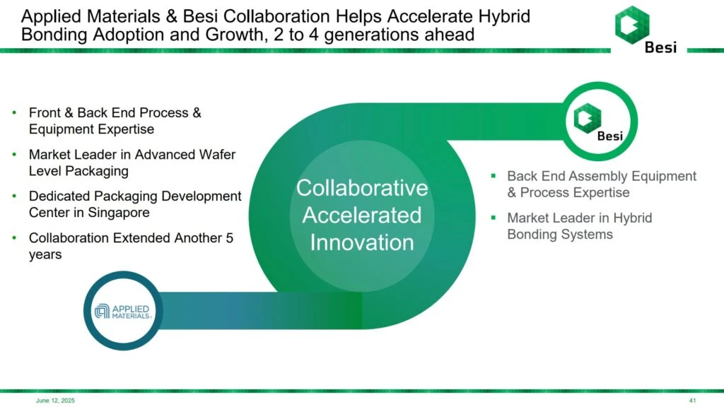
AMAT is a big player in assembly and packaging, as are Lam and Tokyo Electron to a lesser extent. This leaves crumbs left over for BESI, the leader in packaging equipment, and even less so for Kulicke & Soffa (KLIC) and ASMPT (0522, ASMVY).

However, as a leader in advanced packaging, BESI has a super power: It’s had a 5 year-running partnership with AMAT where it gets some additional front-end process step IP to integrate with. And as of this year, AMAT renewed the partnership for another 5 years and backed it up with a more than 9% equity stake in BESI.
So, if you own AMAT, you by extension own a small position in BESI too. This makes for a powerful duo in the emerging advanced packaging space.
Why care about a ~$6 billion semiconductor niche?
Why is the industry suddenly taking more of an interest in the comparatively lo-fi “back-end” chip packaging process steps? In short, it’s because “Moore’s Law” — Intel‘s (INTC) old product roadmap — is dead.
For anyone with doubts about the death of Moore’s Law, the below chart BESI shared explains why. Transistors — the tiny “switches” developed on silicon wafers that eventually create the binary 1s and 0s of software — aren’t scaling like they used to. It’s getting much harder to cram more transistors onto a single chip (left chart in the slide).

Even worse than transistor density slowing down, starting about 2017, the manufacturing cost-per-transistor stopped decreasing and actually started to turn higher. Ask anyone in any manufacturing industry, they’ll tell you rising manufacturing costs are NOT EASY to pass along to customers, especially if you’ve gotten them used to the same or lower cost-per-performance in the past.
Other issues like Nvidia bumping up against chip die size limits (these limits are due to lithography reticle size limitations) and inflation in chemicals the last five years (we’ve had just a bit of global supply chain disruption, right???) are also contributing factors.
Alright alright, we care about chip packaging, but what is it?
Moore’s Law is dead (or maybe to be more fair, it’s slowly dying), thus chip designers and chipmakers are looking to new areas to increase computing performance, power efficiency, and ultimate cost to manufacture. Enter advanced packaging.
“Advanced packaging” is one of those broad terms waved around like a magic wand by some investors. One of our favorite X/Twitter pitches on AMD: “AMD isn’t just designing chips for AI, it’s redefining the whole category using chiplets and advanced packaging superpowers.” Um, no AI chatbot regurgitator, that’s not quite the whole story…
Ok, but what the hell is advanced packaging, and the closely related “chiplets” revolution, exactly?
Put in simple terms, advanced packaging is about finding more precise and more efficient ways to attach chips to the circuit board — or, attaching chips to other chips (chiplet technology) via interconnects and/or 3D stacking (putting multiple chips on top of each other, rather than just side by side).
As companies have begun experimenting away from monolithic SoCs (systems on chip, pictured on the left below) and delve further into chiplet tech (middle and right side of slide), packaging suddenly needs to be more precise. For some packaging, chip placement now needs 100nm (nanometer, 1nm = 1/billionth of a meter, so really really small) or smaller precision. This certainly is not the 3nm (not much bigger than the diameter of a human DNA strand) wafer development precision like at TSMC, but packaging is moving that direction.
Some of BESI’s new machines can now reach 50nm precision, a necessity especially in 3D stacking where the chips must be properly aligned so that the data transfer and power interconnects line up properly.

Who’s who in chip packaging?
This is where things get really interesting, because what used to be an “assembly and packaging” company — or an OSAT, outsourced semiconductor assembly and test company — is changing. And for BESI, that could mean something of a golden (silicon?) age.
The result, according to BESI, could be an unprecedented 5 year growth spurt — hastened on by the rapid advances in AI chips and accelerated computing infrastructure.
And who are BESI’s customers? The big one is of course TSMC with an advanced packaging fab capital expenditure(CapEx, spending on property and equipment) outlay exceeding $30 billion over the next few years. See our video updates last year on TSMC’s purchase of an LCD screen fab for glass substrate packaging, plus the updates last summer regarding Onto Innovation (ONTO), for more. https://www.youtube.com/watch?v=EpJtJNsQPug
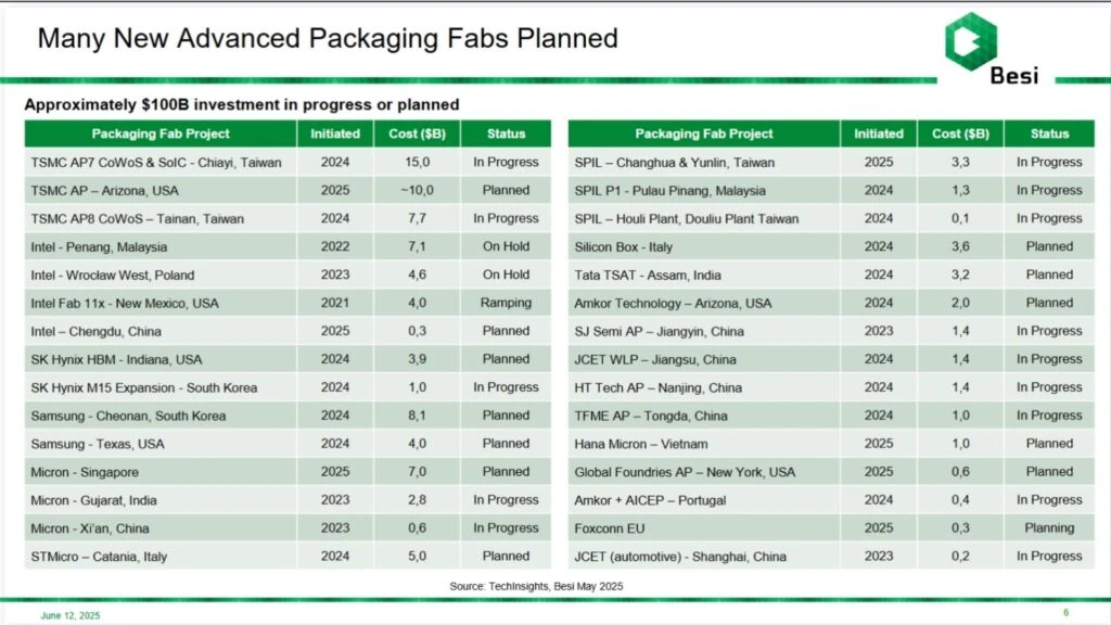
TSMC isn’t alone in investing heavily into advanced packaging, though Intel and Samsung are a distant 2nd and 3rd in CapEx outlay for these new fab projects. We’ve also discussed SK Hynix‘s (000660) work in this area, and then there’s also Micron (MU) and its global expansion plans.
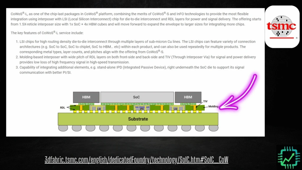
What’s interesting about the above fab packaging list is packaging used to be the domain of the OSATs — like the companies on the right hand side of BESI’s list. But with various packaging technology advancements like TSMC’s CoWoS (Chip-on-Wafer-on-Substrate), some of this packaging can now be efficiently performed directly in a wafer fab.
This may not be great news for the OSATs as their old partners like TSMC may increasingly become competitors. But getting a bunch of new big customers is fantastic for BESI. Check out Semiconductor Insider for more on these advancements.
What does it mean for BESI?
But what does all this chiplet and advanced packaging look like?
BESI provided a diagram of an accelerated compute system to show the different packaging techniques it enables. (If you’re wondering about the below slide, this diagram could be a generalized Broadcom XPU ASIC system, for a customer like Google? It includes the HBM packaged on an electrical interface called an interposer, which in turn is packaged on a substrate.)

Starting in the top left of the slide, hybrid bonding. This is the big packaging technique for BESI, and a key area of growing importance as hybrid bonding enables 3D stacking and other chiplet interconnect packaging (including CPO, so more Nvidia and Broadcom pushing the boundaries of AI data compute). If you zoom in, you can see these hybrid bonds essentially look like tiny microscopic solder balls that enable precise chip placement (as much as 50nm precision) so that the power and data interconnects between chips line up properly.
Moving on, there’s also thermo-compression bonding (TCB), a new area for BESI as Kulicke & Soffa and others already do a lot in TCB. Kind of like how it sounds, TCB involves pressing the two components together (the chip and interposer, for example) and applying heat to create a bond.
And finally there are various types of old “flip-chip” soldering techniques. These are also undergoing a bit of a renaissance, but flip-chip packaging isn’t as precise as hybrid bonding or TCB. And that’s ok. Lots of chips can make due with good ‘ole flip-chip packaging.
BESI has been piling R&D euros into new machines to advance this tech, including in TCB. There’s another new upcoming realm for BESI as well, chiplet molding (bottom right) — the plastic enclosure you’ll see surrounding some of your chips if you’ve ever opened up your computer and peaked at the circuit board. These enclosures also need some advancement, for things like heat dissipation as an example, as chiplet tech and resulting compute performance gets more advanced.

Are you still with us? A few valuation notes
The end result of all this R&D and AI-fueled chip packaging advancement? BESI dramatically raised its financial targets for 2030. The old targets are on the left of the below slide. Revenue was increased by 50% to 90% compared to the previous target, and BESI (in partnership with AMAT) expects to continue to dominate advanced packaging market share.
Pair that with a 5 percentage point raise in expected operating margin, BESI could be a powerful growth engine over the next five year stretch. Remember, the two primary engines of growth are sales and margin, not just sales.

And where is BESI now? Due to the industry downturn, revenue barely topped 600 million euro. So at the high end of the new targets, sales could triple in the next five years. And operating margin at just over 30% has ~10 percentage points or more of possible gains along the way.

The balance sheet is in good shape too, with net cash on balance to help fuel the expected growth. Perhaps a small tuck-in acquisition or two will also aid in the growth? Either way, BESI’s management team has been careful through the industry cycles to keep its net cash balance healthy. The drought the last two years has been especially bad, but the company is still nonetheless in fit and fighting form.
Now the tricky part, about the valuation. At ~55x trailing 12-month earnings per share, BESI is “expensive.” But remember much of this has to do with the cyclical downturn. Cyclical stocks like this almost always look expensive. During cycle bottoms they look expensive because profitability has been clobbered, and during cycle tops it looks expensive because we as collective investors tend to forecast the growth cycle lasting longer than it often will.
However, if we pencil in the 2030 financial targets, assume free cash flow (FCF) can be roughly the same as operating margin (less interest expense), BESI seems to be trading for 10x to 15x 2030 FCF based on the current market cap of $10 billion.
Is the stock a buy? It depends on BESI’s ability to execute on the plan. And besides achieving or exceeding those 2030 financial targets, BESI would only be a good buy if we expect the earnings multiple to stay somewhat elevated by 2030 as well. Maybe not 55x type of elevated, but perhaps 20x to 30x? If so, maybe BESI stock is a double or better in the next five years. Not bad, if you’re looking for market-beating investments.
In other words, while BESI may not be the deal of the decade, it seems there is some value here even after the recovery from the market’s tariff turmoil. Personally, here at CSI we’re content at the moment owning BESI via our large long-time position in AMAT. But if you’re looking for a small-cap bet, give BESI a look. Risks (besides valuation, naturally, seriously we need to stop discussing valuation in isolation from other factors) include BESI’s sub-industry focus on just packaging, AMAT deciding to go a different route at some point in the future, TSMC and other fab’s sensitivity to cost, and of course the semiconductor market sales cycle.
See you over on Semiconductor Insider for more discussion on the topic!
