
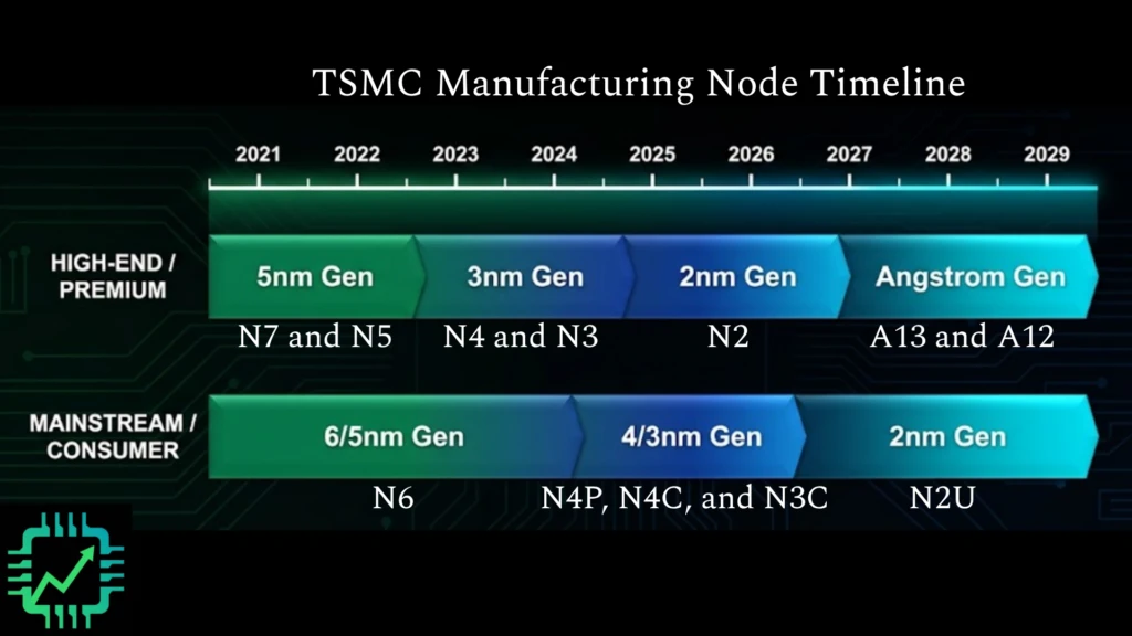
At its North America Technology Symposium this week, Taiwan Semiconductor Manufacturing (TSM) debuted its manufacturing process node through 2029. Last year, TSMC announced its A14 process (the Angstrom process naming lines), which will debut in 2028. This year management announced enhanced versions of A14, dubbed A13 and A12, that will begin production in 2029. This production line is targeted for high-performance applications, including AI data center systems and premium smartphones.
Additionally, the N2 (the nanometer process naming lines) process that is currently ramping up production for 2026, will get a performance upgrade starting in 2028 called N2U. This is a mainstream manufacturing process for mid- to low-end mobile and devices for other mature computing needs. We’ve simplified and generalized the timetable in the chart below. As a reminder, the transistor sizes in the names (nanometers and now Angstroms) no longer reflect actual feature sizes on the chips, but instead are more for marketing and signify higher transistor density compared to past nodes.
You can read TSMC’s press release here: https://pr.tsmc.com/english/news/3302
The big news from this event: TSMC saying ASML’s (ASML) most advanced lithography equipment, high-NA EUV, still isn’t on the roadmap. Though ASML stock fell a bit on TSMC’s discussion, this roadmap isn’t a disaster for the lithography leader. Plenty of litho is still needed as chip demand keeps rising. And ASML is helping its customers make production advancements, like with Nvidia’s (NVDA) cuLitho (computation lithography) announced a few years ago, in production with Nvidia’s EDA software partner/investee Synopsys (SNPS); and ASML’s own investment in frontier AI model startup Mistral AI for enterprise use, including in chip and manufacturing production design speed-up.
However, the semi industry has been clear for several years that lithography process intensity isn’t providing the same computing performance boosts as in decades past. Advanced packaging is the new lowest-hanging-fruit. TSMC has gradually been shifting some of its CapEx to packaging equipment, now up to 10% to 20% of expected capital expenditures (up to $56 billion) for 2026.
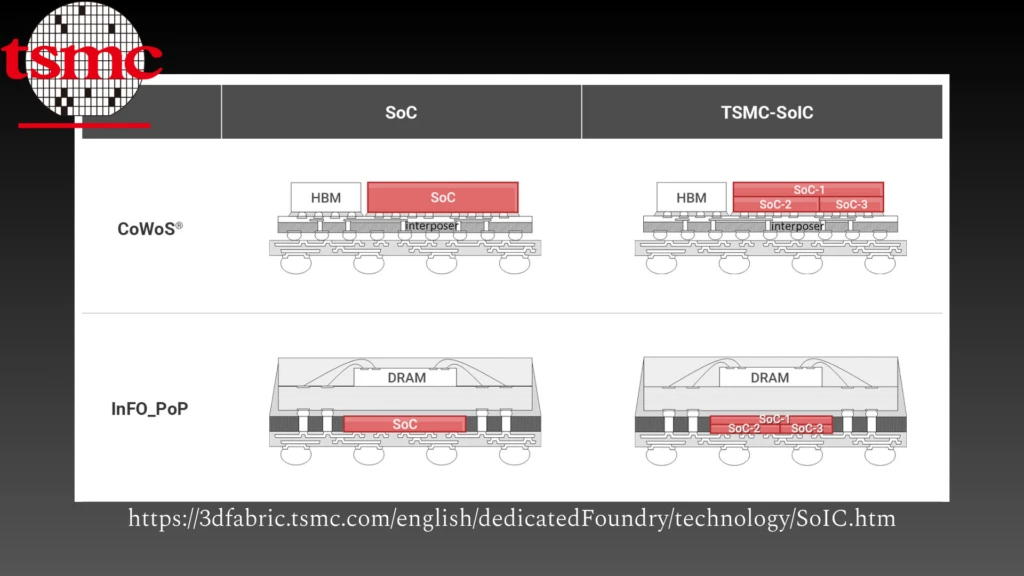
TSMC said its SoIC (System on Integrated Circuit) 3D chiplet-stacking process will come to the A14 node in 2029. COUPE (Compact Universal Photonic Engine) on substrate is also beginning this year, bringing co-packaged optics to AI data center networking.
And on the horizontal (2D) advanced packaging front, TSMC is currently installing a pilot production line for CoPoS (Chip on Panel on Substrate), as mentioned by CEO C.C. Wei on the Q1 2026 earnings call. CoPoS is also expected to head to production within the next few years, succeeding the currently very successful CoWoS (Chip on Wafer on Substrate) packaging processes.
We discussed panel-level packaging a number of times the last couple of years. Here’s one from August 2024:
Among other companies, 3D stacking and panel-level packaging will benefit other companies in the fab equipment space besides ASML, like Applied Materials (AMAT) and its partnership/investment in BE Semiconductor (BESI, OTC:BESIY), and Lam Research (LRCX).
See you on Semi Insider for more on the advanced packaging market! And speaking of chip design, on CSI Live on Wednesday May 6, 8am PT, we’ll be interviewing Faraj Aalaei, former CEO of Aquantia (acquired by Marvell Technology) and now founder of Cognichip, about chip design in the AI era. Come with questions, or submit them via the “Webinars” tab on the Semi Insider Research Dashboard.
